

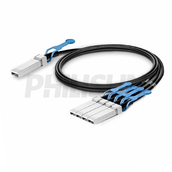
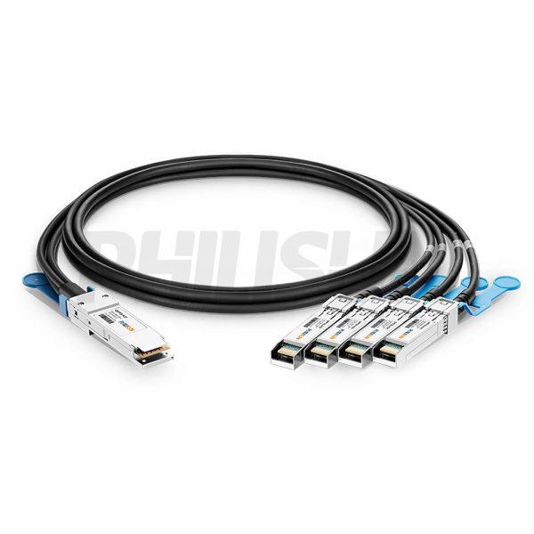
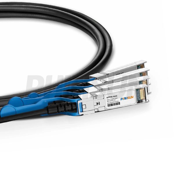
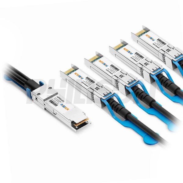
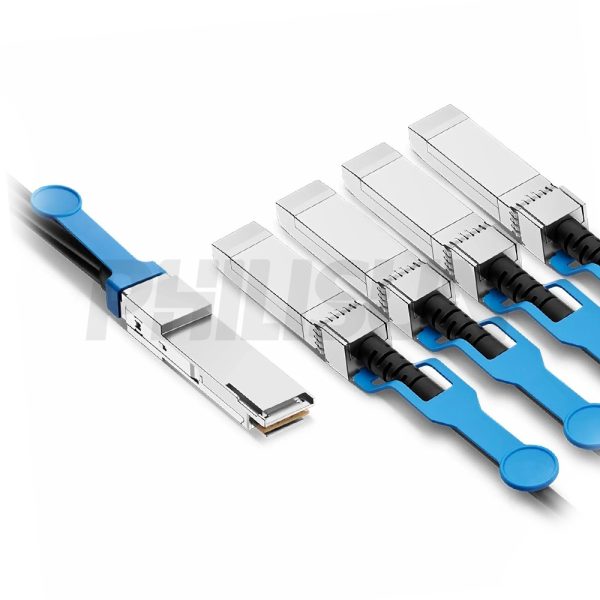
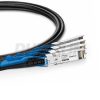


100G QSFP28 to 4×25G SFP28 ACC
Compliant with
QSFP28 MSA, SFP28 MSA, SFF-8665, SFF-8679, SFF-8472, SFF-8402 standard
Switch to Switch
Switch to GPU
- High Quality
- Factory Outlet
- Satisfaction Guarantee
- Global Shipping
| SPECIFICATIONS | |||
|---|---|---|---|
| Cable End Connector A | QSFP28 | Cable End Connector B | 4×SFP28 |
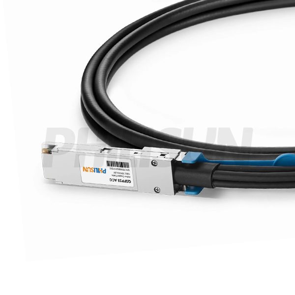
| Jumper Type | Active Optical Breakout Cable | Data Rate | 100G |
| Aggregate Bit Rate | 100Gbps | Lane Bit Rate | 25Gbps |
| Number of Channels | 4 | Single Channel Rate | 10G |
| Minimum Bend Radius | 5X Cable OD -Single, 10X Cable OD - Repeated | Factory Brand | PHILISUN |
| Attenuation | 26AWG:10dB/8.5m maximum 28AWG:10dB/7m maximum 30AWG:8.4dB/5.5m maximum | Bit Error Rate | ≤10-12 |
| Shield | Braid/Foil | Wire AWG | 26AWG/28AWG/30AWG |
| Cable Type | Active Twinax | Cable OD | 30AWG: 6.6mm 28AWG: 8.0mm 26AWG: 8.9mm |
| Cable Colour/Material | Black PVC(OFNR) | Cable Length Selection | 1-9meter |
| Protocols | SFF-8665/SFF-8402/ SFP28 MSA/QSFP28 MSA/SFF-8679/SFF-8472 | Application Scenarios | 100Gigabit Ethernet (100GbE) |
| Supply Voltage | 3.3V | Power Dissipation | <1.8W |
| Operating Temperature | 0 to 70℃ (32 to 158℉) | Storage Temperature | -40 to 85℃ (-40 to 185℉) |
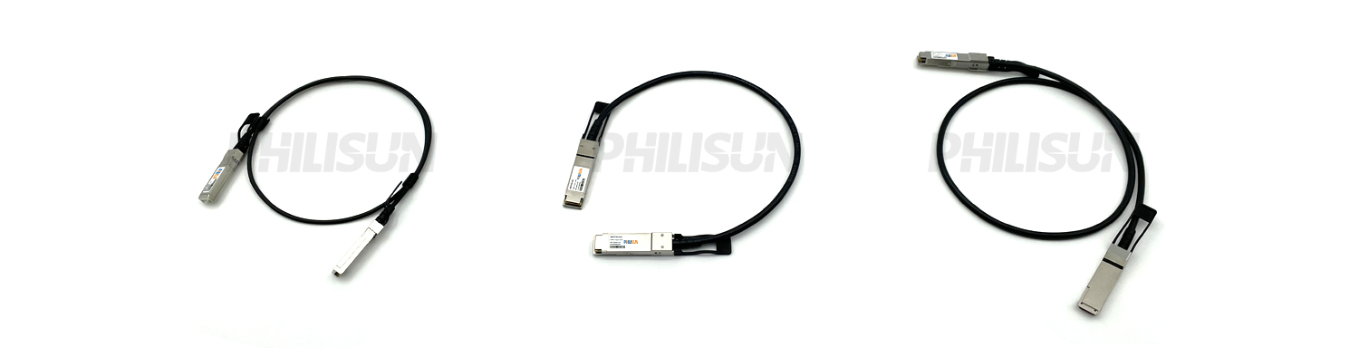
The PHILISUN 100G SFP28 to 4x 25G SFP28 active twinax cable is designed for 100G to 4x 25G Ethernet breakout applications.It complies with SFF-8679, SFF-8472, SFF-8402, SFF-8665, hot-pluggable QSFP28 MSA and SFP28 MSA standards.It connects one 100G QSFP28 port to four 25G SFP28 ports for short‑reach interconnections.Features low latency, low power consumption and high reliability, delivering a cost-effective connectivity solution.Ideal for data centers, high-performance computing (HPC), and intra-rack or adjacent-rack connections for switches, routers, servers and storage systems.

| Absolute Maximum Ratings | |||||||||
| Parameter | Unit | Min. | Typical | Max. | Notes | ||||
| Storage Temperature | ℃ | -40 | – | 85 | – | ||||
| Operating Case Temperature | ℃ | 0 | – | 70 | – | ||||
| Operating Relative Humidity | % | – | – | 85 | – | ||||
| Power Supply Working Voltage | V | 3. 135 | 3 | 3.465 | – | ||||
| Bit Rate | Gbps | – | 100.0 | – | – | ||||
| Electrical Characteristics | |||||||||
| All performance is specified at whole working temperature and conditions | |||||||||
| Item | Parameter | Notes | |||||||
| Physical | Length | 5 m, 6 m, 7 m, 8 m, 9 m | – | ||||||
| – | Cable Colour | Black | – | ||||||
| Electrical | Resistance | 2 ohm Max. | – | ||||||
| – | Insulation Resistance | 10M ohm Min. | – | ||||||
| SI Performance | SDD21 | -22.48d B Min. | @ 12.89GHz | ||||||
| – | SDD11/SDD22 | – 16.5+2*sqrt(f)dB Max. | @0.05GHz-4.1GHz | ||||||
| – | – | – 10.66+ 14*1og(f/5.5)dB Max. | @4. 1GHz- 19GHz | ||||||
| Item | Parameter | Notes | |||||||
| SI Performance | SCD22 | -22+(20/25.78)*f dB Max. | @0.01GHz~ 12.89GHz | ||||||
| – | – 15+(6/25.78)*f dB Max. | @ 12.89GHz~ 19GHz | |||||||
| SCC11 | -2d B Max. | – | |||||||
| SCD21-SDD21 | – 10d B Max. | @0.01GHz~ 12.89GHz | |||||||
| – | -27+(29/22)*f dB Max. | @ 12.89GHz~ 15.7GHz | |||||||
| – | -6.3d B Max. | @ 15.7GHz~ 19GHz | |||||||
| MDNEXT | -30d B Max. | – | |||||||
| COM | 3d B Min. | – | |||||||
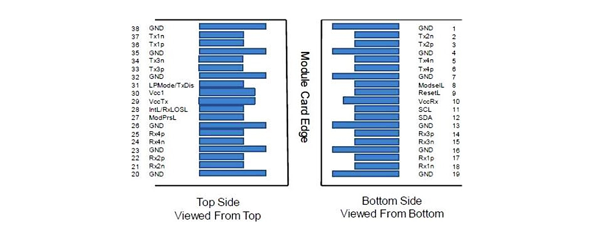
| Pad | Logic | Symbol | Description | Plug Sequence |
|||||
| 1 | – | GND | Ground | 1 | |||||
| 2 | CML-I | Tx2n | Transmitter Inverted Data Input | 3 | |||||
| 3 | CML-I | Tx2p | Transmitter Non-Inverted Data Input | 3 | |||||
| 4 | – | GND | Ground | 1 | |||||
| 5 | CML-I | Tx4n | Transmitter Inverted Data Input | 3 | |||||
| 6 | CML-I | Tx4p | Transmitter Non-Inverted Data Input | 3 | |||||
| 7 | – | GND | Ground | 1 | |||||
| 8 | LVITL-I | ModSeIL | Module Select | 3 | |||||
| 9 | LVITL-I | Resetl | Module Reset | 3 | |||||
| 10 | – | VCCRx | +3.3V Power Supply Receiver | 2 | |||||
| 1 1 | LVCM0S-I/O | SCL | Two-Wire Interface Clock | 3 | |||||
| 12 | LVCM0S-I/O | SDA | Two-Wire Interface Data | 3 | |||||
| 13 | – | GND | Ground | 1 | |||||
| 14 | CML-O | Rx3p | Receiver Non-Inverted Data Output | 3 | |||||
| 15 | CML-O | Rx3n | Receiver Inverted Data Output | 3 | |||||
| 16 | – | GND | Ground | 1 | |||||
| 17 | CML-O | Rx1p | Receiver Non-Inverted Data Output | 3 | |||||
| 18 | CML-O | Rx1n | Receiver Inverted Data Output | 3 | |||||
| 19 | – | GND | Ground | 1 | |||||
| 20 | – | GND | Ground | 1 | |||||
| 21 | CML-O | Rx2n | Receiver Inverted Data Output | 3 | |||||
| 22 | CML-O | Rx2p | Receiver Non-Inverted Data Output | 3 | |||||
| 23 | – | GND | Ground | 1 | |||||
| 24 | CML-O | Rx4n | Receiver Inverted Data Output | 3 | |||||
| 25 | CML-O | Rx4p | Receiver Non-Inverted Data Output | 3 | |||||
| 26 | – | GND | Ground | 1 | |||||
| 27 | LVTTL-O | ModPrsL | Module Present | 3 | |||||
| 28 | LVTTL-O | IntL/ RxL0SL | I nterrupt. Optionaily configurable as RxL0SL via the Management Interface (SFF-8636). |
3 | |||||
| 29 | – | VCCTx | +3.3V Power Supply Transmitter | 2 | |||||
| 30 | – | VCC1 | +3.3V Power Supply | 2 | |||||
| 31 | LVTTL-I | LPMode/Tx Dis | Low Power Mode. Optionally Configurable as Tx Dis via the Management Interface (SFF-8636). |
3 | |||||
| 32 | – | GND | Ground | 1 | |||||
| 33 | CML-I | Tx3p | Transmitter Non-Inverted Data Input | 3 | |||||
| 34 | CML-I | Tx3n | Transmitter Inverted Data Input | 3 | |||||
| 35 | – | GND | Ground | 1 | |||||
| 36 | CML-I | Tx1p | Transmitter Non-Inverted Data Input | 3 | |||||
| 37 | CML-I | Tx1n | Transmitter Inverted Data Input | 3 | |||||
| 38 | – | GND | Ground | 1 | |||||
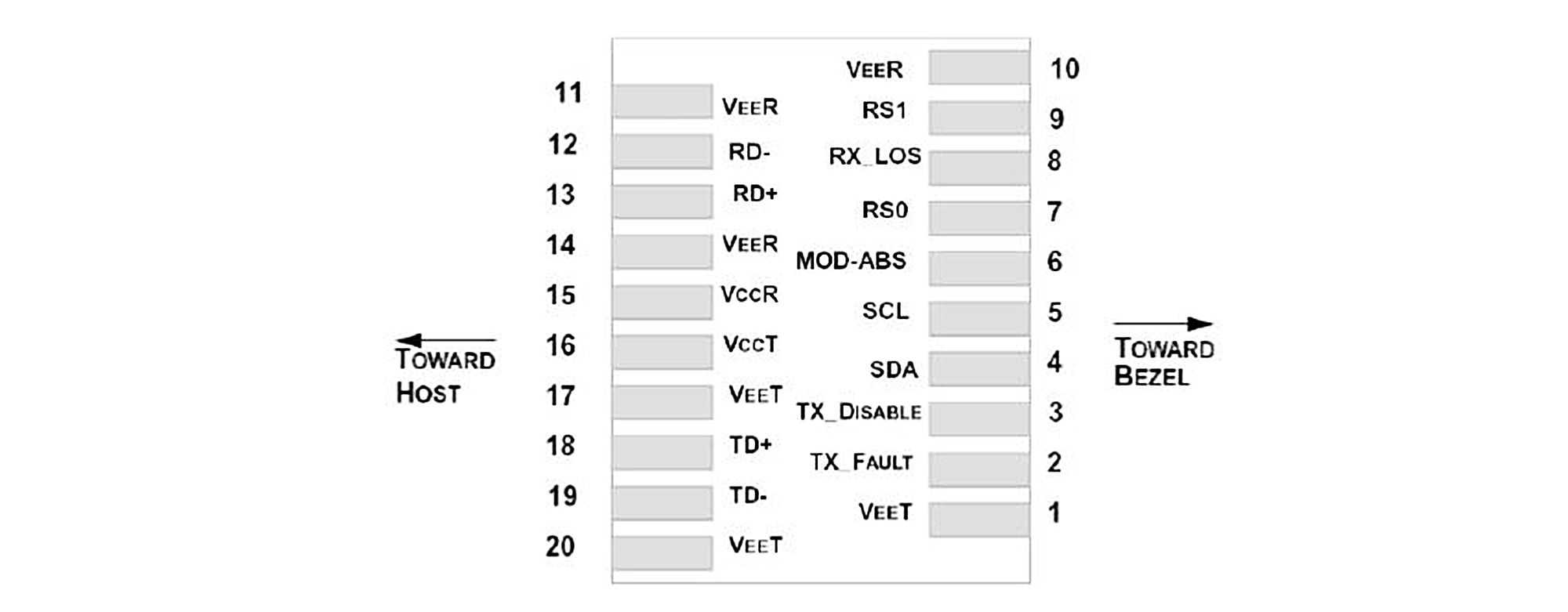
| Pin No. | Symbol | Level/Logic | Description | ||||||
| 1 | VEET | – | Module Transmitter Ground | ||||||
| 2 | TX_FAULT | LVTTL-O | Module Transmitter Fault Indication | ||||||
| 3 | TX_DIS | LVTTL-I | Transmitter Disable; Active High Disable Transmitter Output | ||||||
| 4 | SDA | LVTTL-I | 2-Wire Serial Interface Data Line | ||||||
| 5 | SCL | LVTTL-I/O | 2-Wire Serial Interface Clock | ||||||
| 6 | MOD_ABS | LVTTL-O | Module A bsent. Connected to Ground in the Module | ||||||
| 7 | RS0 | – | Rate Select 0. Optionally Controls SFP28 Module Receiver | ||||||
| 8 | RX_LOS | LVTTL-O | Loss of Receiver Signal Indication | ||||||
| 9 | RS1 | – | Rate Select 1, Optionally Controls SFP28 Module Transmitter | ||||||
| 10 | VEER | – | Module Receiver Ground | ||||||
| 11 | VEER | – | Module Receiver Ground | ||||||
| 12 | RD- | CML-O | Receiver Inverted Data Output | ||||||
| 13 | RD+ | CML-O | Receiver Non-Inverted Data Output | ||||||
| 14 | VEER | – | Module Receiver Ground | ||||||
| 15 | VCCR | – | Module Receiver 3.3V Supply | ||||||
| 16 | VCCT | – | Module Transmitter 3.3V Supply | ||||||
| 17 | VEET | – | Module Transmitter Ground | ||||||
| 18 | TD+ | CML-I | Transmitter Non-Inverted Data Input | ||||||
| 19 | TD- | CML-I | Transmitter Inverted Data Input | ||||||
| 20 | VEET | – | Module Transmitter Ground | ||||||

Related products
-
")
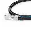
100G QSFP28 to 2×50G QSFP28 Active Direct Attach Copper Twinax Cable (ACC)
Compliant with
SFF-8665, QSFP28 MSA, SFF-8636, SFF-8679 standard
Switch to Switch
Switch to GPU