

-600x600.jpg)
-600x600.jpg)
-600x600.jpg)
-600x600.jpg)
-600x600.jpg)
-100x100.jpg)
-100x100.jpg)
-100x100.jpg)
-100x100.jpg)
-100x100.jpg)
200G QSFP56 to 2×100G QSFP56 Active Optical Cable(AOC)
Compliant with the SFF-8665 QSFP56 MSA standard
Switch to Switch
Switch to GPU
- High Quality
- Factory Outlet
- Satisfaction Guarantee
- Global Shipping
| SPECIFICATIONS | |||
|---|---|---|---|
| Cable End Connector A | QSFP56 | Cable End Connector B | 2×QSFP56 |
| Jumper Type | Active Optical Breakout Cable | Data Rate | 200G |
| Aggregate Bit Rate | 212.5Gbps | Lane Bit Rate | 53.125Gbps |
| Number of Channels | 4 | Single Channel Rate | 50G |
| Array Transmitter | VSCEL | Array Receiver | PIN |
| Minimum Bend Radius | 30mm | Factory Brand | PHILISUN |
| Center(Operating) Wavelength | 850nm | Bit Error Rate | 2.4E-4 |
| Fiber Type | OM3 MMF MAX 70m | Cable Colour | Aqua |
| Cable Material | LSZH/OFNP | Cable Length Selection | 1-70meter |
| Safety Certification | TUV/UL/FDA | Application Scenarios | 200 Gigabit Ethernet (200GbE) |
| Protocols | IEEE 802.3,QSFP56 MSA,SFF-8024,SFF-8679,SFF-8665,SFF-8636 | DDMI(Commercial) | YES |
| Supply Voltage | 3.3V | Power Dissipation | <4.5W |
| Operating Temperature | 0 to 70℃ (32 to 158℉) | Storage Temperature | -20 to 85℃ (-4 to 185℉) |
PRODUCT PRESENTATION
This QSFP56 to 2×100G QSFP56 breakout active optical cable uses multi‑mode fiber (MMF).It complies with IEEE 802.3, QSFP56 MSA, SFF-8024, SFF-8679, SFF-8665, and SFF-8636.It links one 200G QSFP56 port to two 100G QSFP56 ports, ideal for high‑speed connections within and between adjacent racks.
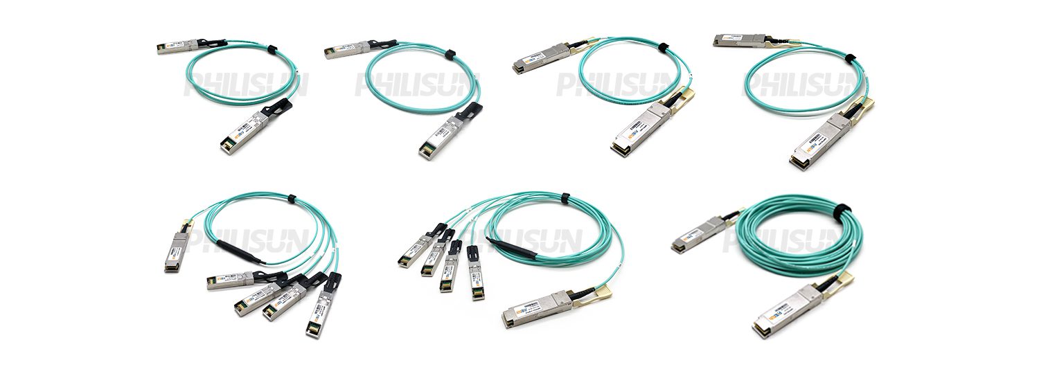
AOC SERIES PRODUCTS
PRODUCTION & TESTING EQUIPMENT

PERFORMANCE PARAMETER
| Absolute Maximum Ratings | |||||||||
| Parameter | Symbol | Min | Typical | Max | Unit | ||||
| Storage Temperature | TS | -20 | – | 85 | ℃ | ||||
| Relative Humidity | RH | 0 | – | 85 | % | ||||
| Case Operating Temperature | TCase | 0 | – | 70 | ℃ | ||||
| Supply Voltage | VCC | -0.5 | – | 3.6 | V | ||||
| Transmitter Specifications | |||||||||
| Parameter | Symbol | Min. | Typ. | Max. | Unit | ||||
| Signaling Speed per Lane | PRBS31Q@26.5625Gbd PAM4 | Gb/s | |||||||
| Center Wavelength | C | 840 | 850 | 860 | nm | ||||
| Differential Input Impedance | Zin | 90 | 100 | 110 | Ohm | ||||
| Differential Input Voltage | Vin | – | 900 | – | mVp-p | ||||
| Differential termination mismatch | – | – | – | 10 | % | ||||
| DC common mode voltage | – | -350 | – | 2850 | mV | ||||
| Receiver Specifications | |||||||||
| Parameter | Symbol | Min. | Typ. | Max. | Unit | ||||
| Signaling Speed per Lane | PRBS31Q@26.5625Gbd PAM4 | Gb/s | |||||||
| Center Wavelength | C | 840 | 850 | 860 | nm | ||||
| Differential Input Impedance | – | – | – | 10 | % | ||||
| Differential Input Voltage | Zout | 90 | 100 | 110 | Ohm | ||||
| Differential termination mismatch | Vout | – | – | 900 | mVp-p | ||||
| DC common mode voltage | – | -350 | – | 2850 | mV | ||||
| Error Bit Rate | BER | – | – | 2.4E-4 | PRBS31Q@26.5 625Gbd PAM4 |
||||
| Recommended Operating Environment | |||||||||
| Parameter | Symbol | Min | Typical | Max | Unit | ||||
| Power Supply Voltage | VCC | 3.135 | 3.300 | 3.465 | V | ||||
| Operating Case Temperature | TC | 0 | 25 | 70 | ℃ | ||||
| Power dissipation (200G retiming on all lanes) |
Pd200G | – | – | 4.5 | W | ||||
| Power dissipation (100G retiming on all lanes) |
Pd100G | – | – | 2.5 | W | ||||
PIN DESCRIPTIONS
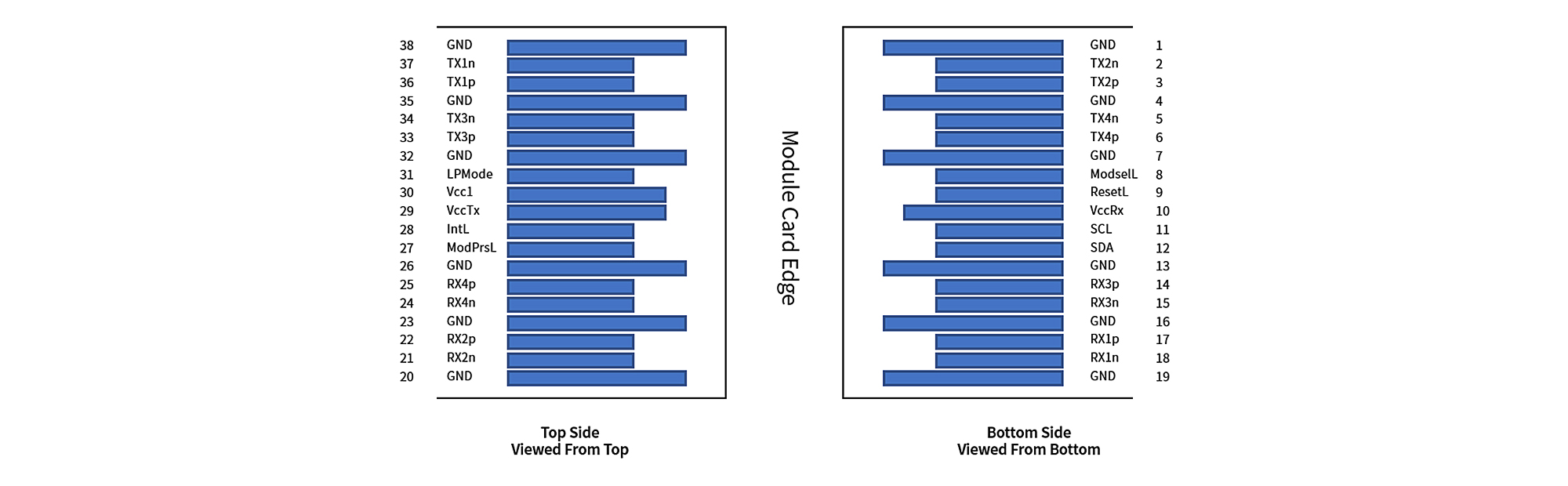
PIN DEFINITION RECEIVER SPECIFICATIONS
| Pin | Symbol | Name/Description | |||||||
| 1 | GND | Ground | |||||||
| 2 | Tx2n | Transmitter Inverted Data Input | |||||||
| 3 | Tx2p | Transmitter Non-Inverted Data Input | |||||||
| 4 | GND | Ground | |||||||
| 5 | Tx4n | Transmitter Inverted Data Input | |||||||
| 6 | Tx4p | Transmitter Non-Inverted Data Input | |||||||
| 7 | GND | Ground | |||||||
| 8 | ModSelL | Module Select | |||||||
| 9 | ResetL | Module Reset | |||||||
| 10 | Vcc Rx | +3.3 V Power supply receiver | |||||||
| 11 | SCL | 2-wire serial interface clock | |||||||
| 12 | SDA | 2-wire serial interface data | |||||||
| 13 | GND | Ground | |||||||
| 14 | Rx3p | Receiver Non-Inverted Data Output | |||||||
| 15 | Rx3n | Receiver Inverted Data Output | |||||||
| 16 | GND | Ground | |||||||
| 17 | Rx1p | Receiver Non-Inverted Data Output | |||||||
| 18 | Rx1n | Receiver Inverted Data Output | |||||||
| 19 | GND | Ground | |||||||
| 20 | GND | Ground | |||||||
| 21 | Rx2n | Receiver Inverted Data Output | |||||||
| 22 | Rx2p | Receiver Non-Inverted Data Output | |||||||
| 23 | GND | Ground | |||||||
| 24 | Rx4n | Receiver Inverted Data Output | |||||||
| 25 | Rx4p | Receiver Non-Inverted Data Output | |||||||
| 26 | GND | Ground | |||||||
| 27 | ModPrsL | Module Present | |||||||
| 28 | IntL | Interrupt | |||||||
| 29 | Vcc Tx | +3.3 V Power supply transmitter | |||||||
| 30 | Vcc1 | +3.3 V Power Supply | |||||||
| 31 | LPMode | Low Power Mode | |||||||
| 32 | GND | Ground | |||||||
| 33 | Tx3p | Transmitter Non-Inverted Data Input | |||||||
| 34 | Tx3n | Transmitter Inverted Data Input | |||||||
| 35 | GND | Ground | |||||||
| 36 | Tx1p | Transmitter Non-Inverted Data Input | |||||||
| 37 | Tx1n | Transmitter Inverted Data Input | |||||||
| 38 | GND | Ground | |||||||
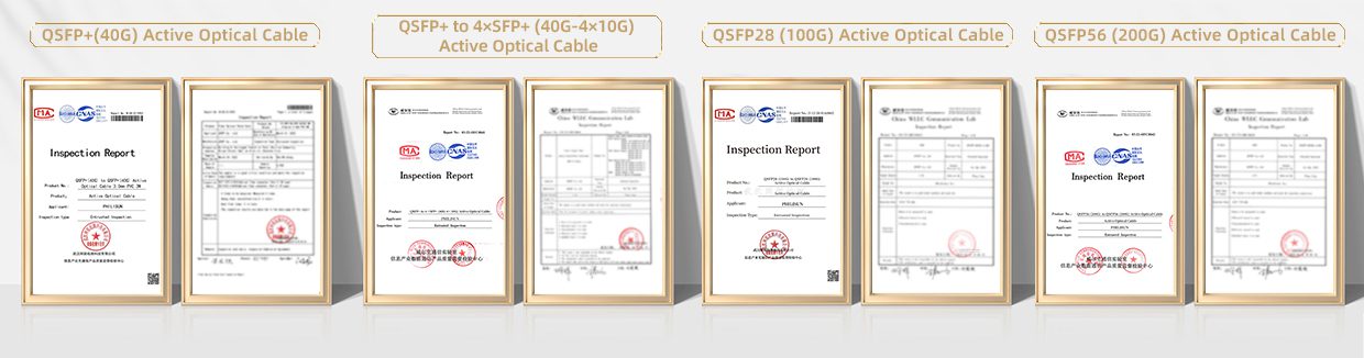
PRODUCT CERTIFICATION
COMPATIBLE BRANDS

CONFIGURATION INFORMATION
Related products
-
")
200G QSFP56 to QSFP56 Active Optical Cable (AOC)
Compliant with theSFF-8436 QSFP56 MSA standard
Switch to Switch
Switch to GPU -
")
200G QSFP56 to 4×50G SFP56 Active Optical Cable(AOC)
Compliant with the SFF-8436 QSFP56 MSA standard
Switch to Switch
Switch to GPU