

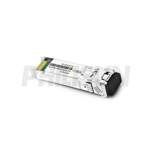
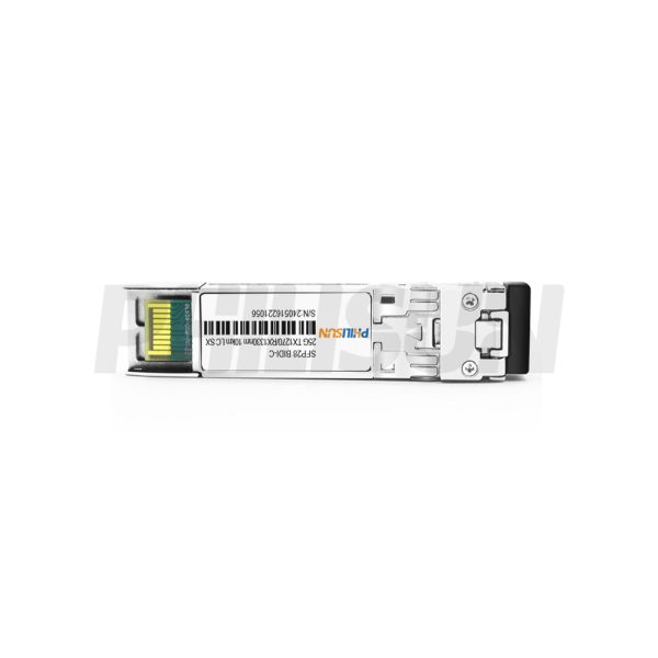
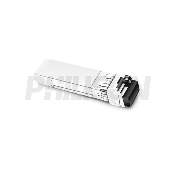
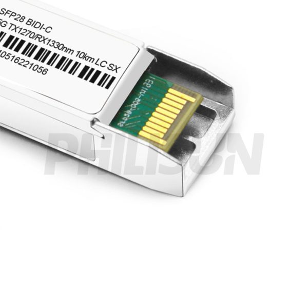
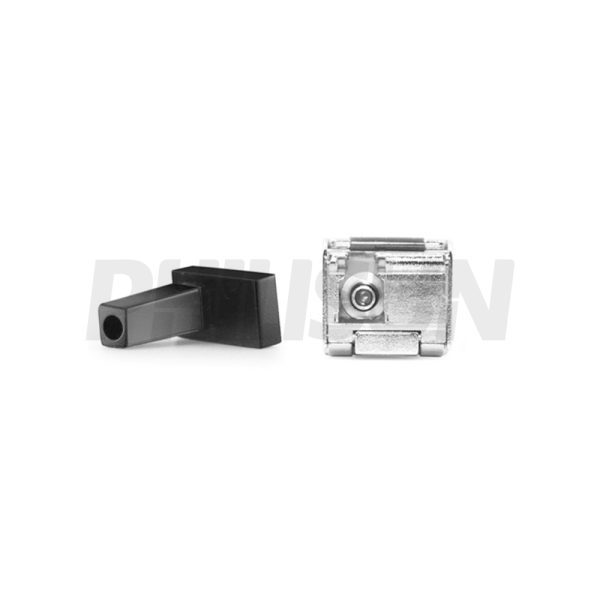
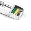
25G LR SFP28 BIDI 1270/1330nm 10km DOM Simplex LC SMF Transceiver
SFP28BD-25-1213-10(LR)-LC
- High Quality
- Factory Outlet
- Satisfaction Guarantee
- Global Shipping
| SPECIFICATIONS | |||
|---|---|---|---|
| Product Model | SFP28BD-25-1213-10(LR)-LC | Manufacturer Brand | PHILISUN |
| Package Type | SFP28 | Optical Connector | LC |
| Max Data Rate | 25.78Gbps | Channel Data Rate | - |
| Effective Transmission Distance | 10km | ||
| Wavelength | 1270nm-TX/1330nm-RX | Operating Voltage | 3.3V |
| Fiber Type | SMF | Core Size | 9/125µm |
| Transmitter Type | DFB BiDi | Receiver Type | PIN |
| TX Power | -2~4dBm | Receiver Sensitivity | <-13dBm |
| Digital Optical Monitoring(DOM) | YES | Receiver Overload | 2dBm |
| Power Consumption | ≤1W | Protocols | MSA, CPRI, eCPRI |
| Operating Temperature(Commercial) | 0℃~+70℃ | Storage Temperature(Commercial) | -40℃~+85℃ |
PRODUCT PRESENTATION
The PHILISUN SFP28 BIDI 25G 1270/1330nm 10km LR LC SX transceivers are high-performance modules designed for Ethernet links, supporting data rates of up to 25.78Gbps and transmission distances of up to 10km. These transceivers are compliant with SFF-8472 and are compatible with SFF-8432 and relevant parts of SFF-8431 standards.Additionally, the product meets RoHS compliance and is lead-free, adhering to Directive 2011/96/EU, making it an environmentally friendly and reliable solution for high-speed networking applications.
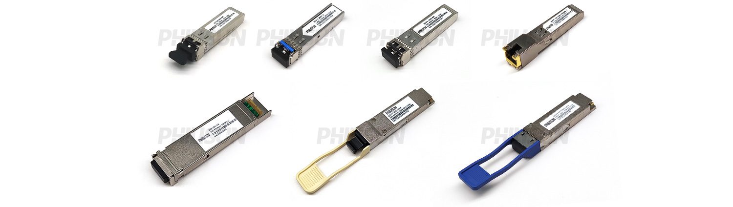
TRANSCEIVER SERIES PRODUCTS
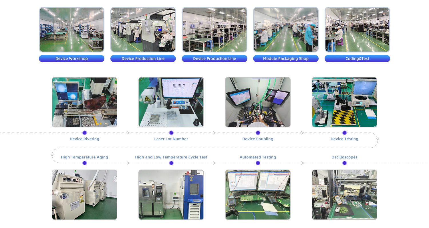
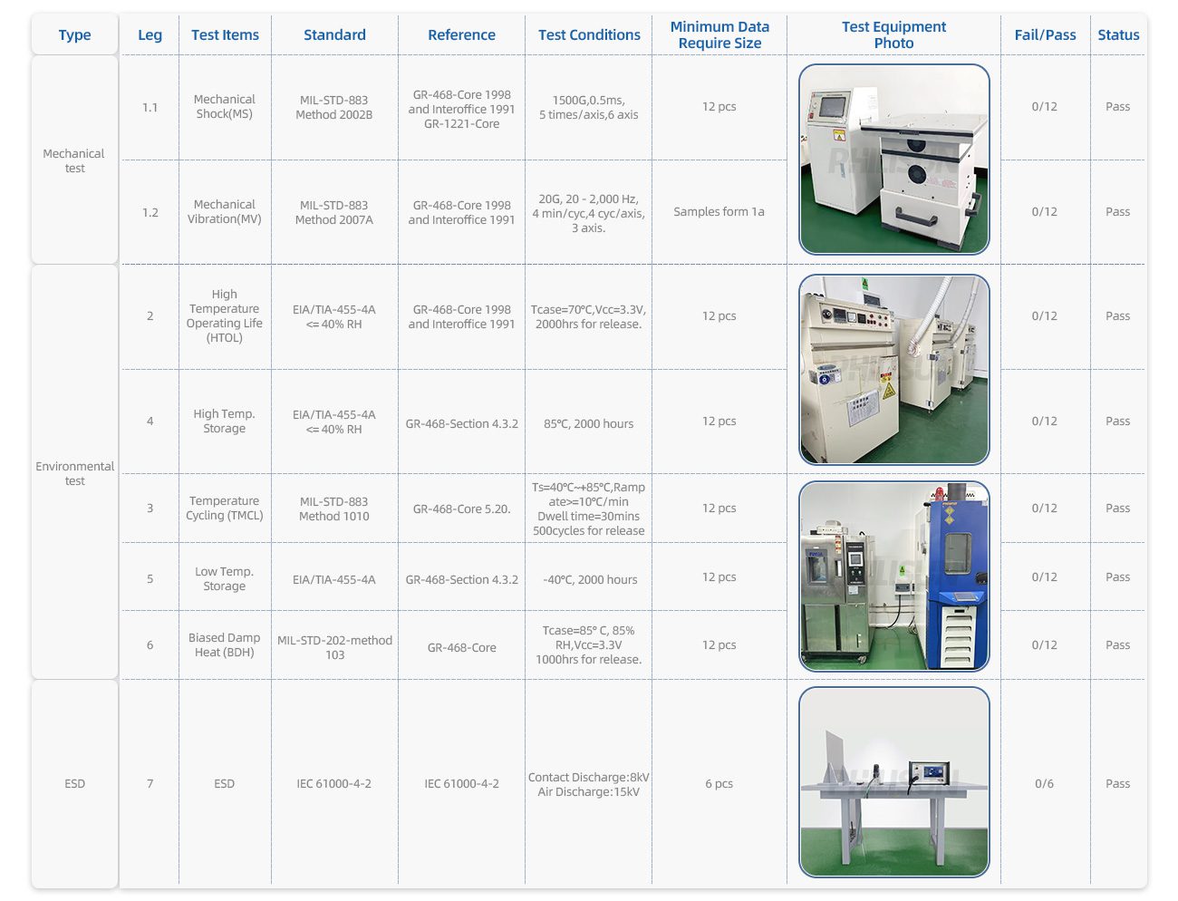
PRODUCTION & TESTING EQUIPMENT
PERFORMANCE PARAMETER
| General Specifications | |||||||||
| Parameter | Symbol | Min. | Typ. | Max. | Unit | Note | |||
| Transmitter | |||||||||
| Center Wavelength | λt | 1265 | 1271 | 1277 | nm | – | |||
| 1325 | 1331 | 1337 | nm | – | |||||
| spectral width(-20dB) | △λ | – | – | 1 | nm | – | |||
| Average optical Power | Pavg | -5.0 | – | 2 | dBm | 1 | |||
| Laser off power | Poff | – | – | -30 | dBm | – | |||
| Side mode suppression ratio | – | 30 | – | – | – | – | |||
| Extinction ratio | ER | 3.5 | – | – | dB | – | |||
| Optical return loss tolerance | – | – | – | -12 | dB | – | |||
| Receiver | |||||||||
| Center wavelength | λr | 1325 | 1331 | 1337 | nm | – | |||
| 1265 | 1271 | 1277 | nm | – | |||||
| Receiver sensitivity | Sen | – | – | -9 | dB | 2 | |||
| Los assert | LOSA | -30 | – | – | dBm | – | |||
| Los dessert | LOSD | – | – | -16 | dBm | – | |||
| Los hysteresis | LOSH | 0.5 | – | – | dB | – | |||
| Overload | – | 2 | – | – | dBm | – | |||
| Notes: 1. Average power figures are informative only, per IEEE802.3cc. 2. Receiver sensitivity is informative. Shall be measured with conformance test signal for . BER =5x 10⁻⁵ . |
|||||||||
| Absolute Maximum Ratings | |||||||||
| Parameter | Symbol | Min. | Typ. | Max. | Unit | Note | |||
| Maximum supply voltage | Vcc | 0 | – | 3.6 | V | – | |||
| Storage temperature | TS | -40 | – | 85 | °C | – | |||
| Case operating temperature | TA | 0 | – | 70 | °C | Commercial | |||
| Relative humidity | RH | 0 | – | 85 | % | 1 | |||
| Notes: Non-condensing. | |||||||||
| Electrical Characteristics | |||||||||
| Parameter | Symbol | Min. | Typ. | Max. | Unit | Note | |||
| Supply voltage | VCC | 3.14 | – | 3.46 | V | – | |||
| Supply current | Icc | – | – | 300 | mA | Commercial | |||
| 360 | mA | Extended | |||||||
| 360 | mA | Industrial | |||||||
| Power consumption | P | – | – | 1 | W | Commercial | |||
| 1.2 | W | Extended | |||||||
| 1.2 | W | Industrial | |||||||
| Data rate | R | 24.3 | – | 26.5 | Gb/s | – | |||
| Fiber Length | L | – | – | 10 | KM | – | |||
| Transmitter (Tx) | |||||||||
| Input differential impedance | Rin | – | 100 | – | Ω | 1 | |||
| Differential data input swing | Vin,pp | 180 | – | 700 | mV | 2 | |||
| Transmit disable voltage | VD | 2 | – | Vcc | V | – | |||
| Transmit enable voltage | VEN | Vee | – | Vee+0.8 | V | – | |||
| Receiver (Rx) | |||||||||
| Single ended output voltage tolerance |
V | -0.3 | – | 4 | V | – | |||
| Rx output diff voltage | Vo | 180 | – | 450 | mV | – | |||
| LOS fault | VLOS fault | 2 | – | VccHOST | V | 4 | |||
| LOS normal | VLOS norm | Vee | – | Vee+0.8 | V | 4 | |||
| Notes: 1.Connected directly to TX data input pins. AC coupling from pins into laser driver IC. 2.Per SFF-8431 Rev 3.0 3.Into 100 ohms differential termination. 4.LOS is an open collector output. Should be pulled up with 4.7kΩ – 10kΩ on the host board. Normal operation is logic 0; loss of signal is logic 1. Maximum pull-up voltage is 5.5V. |
|||||||||
| Optical Characteristics | |||||||||
| Parameter | Symbol | Min. | Typ. | Max | Unit | Notes | |||
| Transmitter (Tx) | |||||||||
| Center wavelength | λt | 1295 | 1271 | 1277 | nm | – | |||
| 1325 | 1331 | 1337 | nm | – | |||||
| Average optical power | PAVE | -2 | – | 4 | dBm | 1 | |||
| Spectral width(-20dB) | △λ | – | – | 1 | nm | – | |||
| Laser off power | Poff | – | – | -30 | dBm | – | |||
| Side mode suppression ratio | – | 30 | – | – | – | – | |||
| Extinction ratio | ER | 3.5 | – | – | dB | – | |||
| Optical return loss tolerance | – | – | – | -12 | dB | – | |||
| Receiver (Rx) | |||||||||
| Center wavelength | λr | 1325 | 1331 | 1337 | nm | – | |||
| 1265 | 1271 | 1277 | nm | – | |||||
| Receiver sensitivity | Sen | – | – | -13 | dBm | 2 | |||
| Overload | – | 2 | – |
–
|
dBm | 2 | |||
| LOS de-assert | LOSA | – |
–
|
-14 | dBm | – | |||
| Los assert | LOSA | -30 | -23 | – | dBm | – | |||
| Los hysteresis | – | 0.5 | – |
–
|
dB | – | |||
| Notes: 1.Average Power figures are informative only, per IEEE802.3cc. 2.Receiver sensitivity is informative. Shall be measured with conformance test signal for . BER =5x 10⁻⁵ . |
|||||||||
| Digital Diagnostic Specifications | |||||||||
| Parameter | Symbol | Units | Min. | Max. | Accuracy | Note | |||
| Transceiver temperature | T | – | 0 | +70 | ±5 ºC | Commercial | |||
| Transceiver supply voltage | DDVoltage | V | 3.15 | 3.15 | ±3% | – | |||
| Transmitter bias current | DDBias | mA | 0 | 35 | ±10% | – | |||
| Transmitter output power | DDTx-Power | dBm | -5 | +5 | ±3dB | – | |||
| Receiver average optical input power | DDRx-Power | dBm | -16 | -3 | ±3dB | – | |||
| Timing Characteristics | |||||||||
| Parameter | Symbol | Min. | Typ. | Max. | Unit | ||||
| TX_disable assert time | t_off | – | – | 100 | us | ||||
| TX_disable negate time | t_on | – | – | 2 | ms | ||||
| Time to initialize 2-wire interface | t_2w_start_up | – | – | 300 | ms | ||||
| Time to initialize | t_start_up | – | – | 300 | ms | ||||
| Time to initialize cooled module and time to power up a cooled module to power level II | t_start_up_cooled | – | – | 90 | s | ||||
| Time to power up to level II | t_power_level2 | – | – | 300 | ms | ||||
| Time to power down from level II | t_power_down | – | – | 300 | ms | ||||
| Tx_fault assert | Tx_Fault_on | – | – | 1 | ms | ||||
| Tx_fault assert for cooled module | Tx_Fault_on_cooled | – | – | 50 | ms | ||||
| TX_FAULT reset | t_reset | 10 | – | – | us | ||||
| Rx_LOS assert delay | t_los_on | – | – | 100 | us | ||||
| Rx_LOS negate delay | t_los_off | – | – | 100 | us | ||||
PIN DESCRIPTION
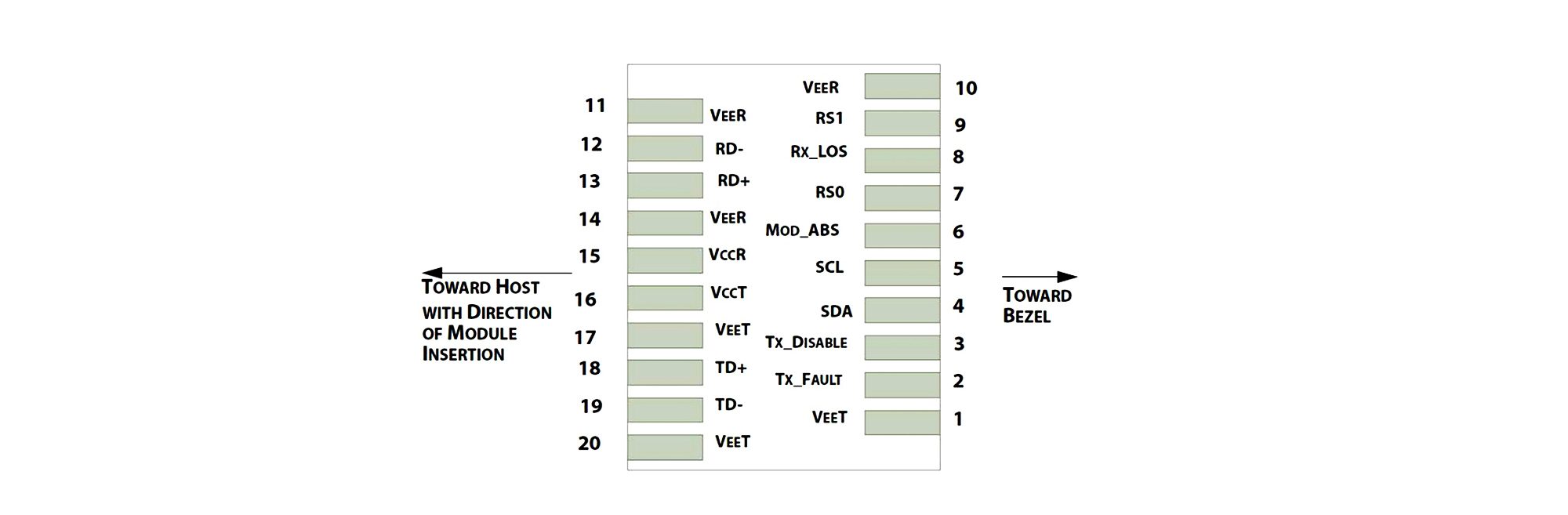
| Pin | Symbol | Name/Description | Plug Seq. | ||||||
| 1 | VeeT | Module transmitter ground | 1 | ||||||
| 2 | TX fault | Module transmitter fault | 2 | ||||||
| 3 | TX disable | Transmitter disable; turns off transmitter laser output | 3 | ||||||
| 4 | SDL | 2 wire serial interface data input/output (SDA) | 4 | ||||||
| 5 | SCL | 2 wire serial interface clock input (SCL) | 4 | ||||||
| 6 | MOD_ABS | Module absent, connect to VeeR or VeeT in the module | 2 | ||||||
| 7 | RS0 | Rate select0: module inputs and are pulled low to VeeT with > 30kΩ resistorsin the module. | – | ||||||
| 8 | LOS | Receiver Loss of signal indication | – | ||||||
| 9 | RS1 | Rate select1: module inputs and are pulled low to VeeT with > 30kΩ resistorsin the module. | – | ||||||
| 10 | VeeR | Module receiver ground | 1 | ||||||
| 11 | VeeR | Module receiver ground | 1 | ||||||
| 12 | RD- | Receiver inverted data out put | – | ||||||
| 13 | RD+ | Receiver non-inverted data out put | – | ||||||
| 14 | VeeR | Module receiver ground | 1 | ||||||
| 15 | VccR | Module receiver 3.3V supply | – | ||||||
| 16 | VccT | Module transmitter 3.3V supply | – | ||||||
| 17 | VeeT | Module transmitter ground | 1 | ||||||
| 18 | TD+ |
Transmitter non-inverted data out put
|
– | ||||||
| 19 | TD- | Transmitter inverted data out put | – | ||||||
| 20 | VeeT | Module transmitter ground | 1 | ||||||
| Notes: 1.The module ground pins shall be isolated from the module case. 2.This pin is an open collector/drain output pin and shall be pulled up with 4.7K-10Kohms to Host_Vcc on the host board. 3.This pin shall be pulled up with 4.7K-10Kohms to VccT in the module. 4.This pin is an open collector/drain output pin and shall be pulled up with 4.7K-10Kohms to Host_Vcc on the host board. |
|||||||||
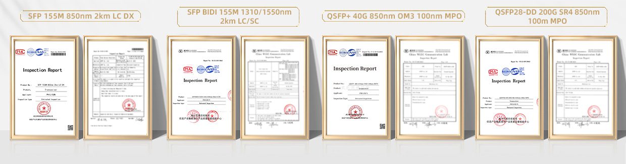
PRODUCT CERTIFICATION
QUALITY ADVANTAGE
COMPATIBLE BRANDS

CONFIGURATION INFORMATION
Related products
-
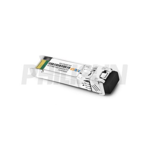
25G ELR SFP28 BIDI 1270/1330nm 20km DOM Simplex LC SMF Transceiver
SFP28BD-25-1213-20(ELR)-LC