

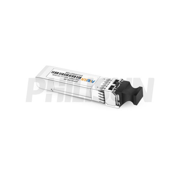
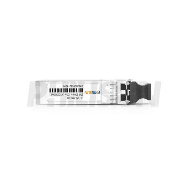
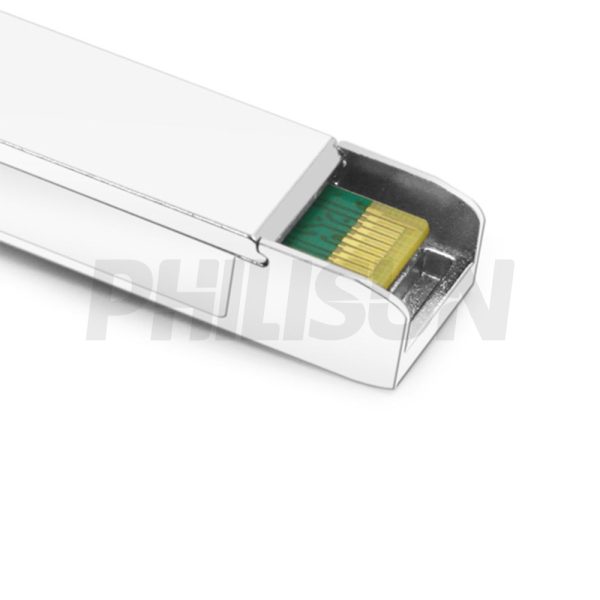
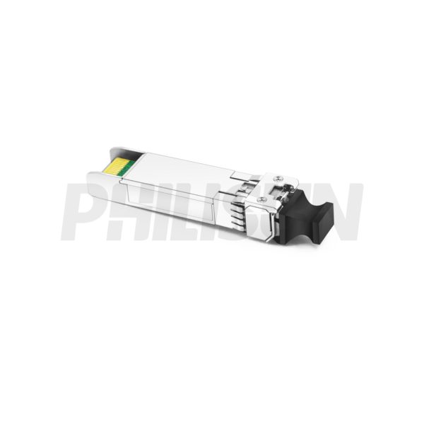
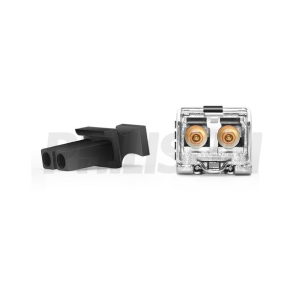
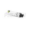
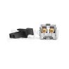
25GBASE-SR SFP28 850nm 100m DOM Duplex LC MMF Transceiver
SFP28-25-85-01(SR)-LCD
- High Quality
- Factory Outlet
- Satisfaction Guarantee
- Global Shipping
| SPECIFICATIONS | |||
|---|---|---|---|
| Product Model | SFP28-25-85-01(SR)-LCD | Manufacturer Brand | PHILISUN |
| Package Type | SFP28 | Optical Connector | Duplex LC |
| Max Data Rate | 25.78G | Channel Data Rate | 10.31Gbps |
| Effective transmission distance(OM3) | 70m | Effective transmission distance(OM4) | 100m |
| Wavelength | 850nm | Operating Voltage | 3.3V |
| Fiber Type | MMF | Core Size | 50/125µm |
| Transmitter Type | VCSEL | Receiver Type | PIN |
| TX Power | -8.4~2.4dbm | Receiver Sensitivity | <-6dBm |
| Digital Diagnostic Monitoring(DDM) | YES | Receiver Overload | 2.4dBm |
| Power Consumption | <1.0W | Protocols | SFF-8472, SFF-8024, SFF-8431, SFF-8432 |
| Operating temperature(Commercial) | 0℃~+70℃ | Storage Temperature(Commercial) | -40℃~+85℃ |
| Operating temperature(Industrial) | -40℃~+85℃ | Storage Temperature(Industrial) | -40℃~+85℃ |
PRODUCT PRESENTATION
The PHILISUN SFP28 25G 850nm 100m SR LC DX transceiver is optimized for 25.78Gbps data transmission over multimode fiber. Fully compliant with the SFF-8431 standard, its SFP+ mechanical design is compatible with the SFF-8432 specification.This module supports digital diagnostic monitoring through a 2-wire serial interface, as outlined in the SFF-8472 standard, ensuring precise performance monitoring and simplified network management.
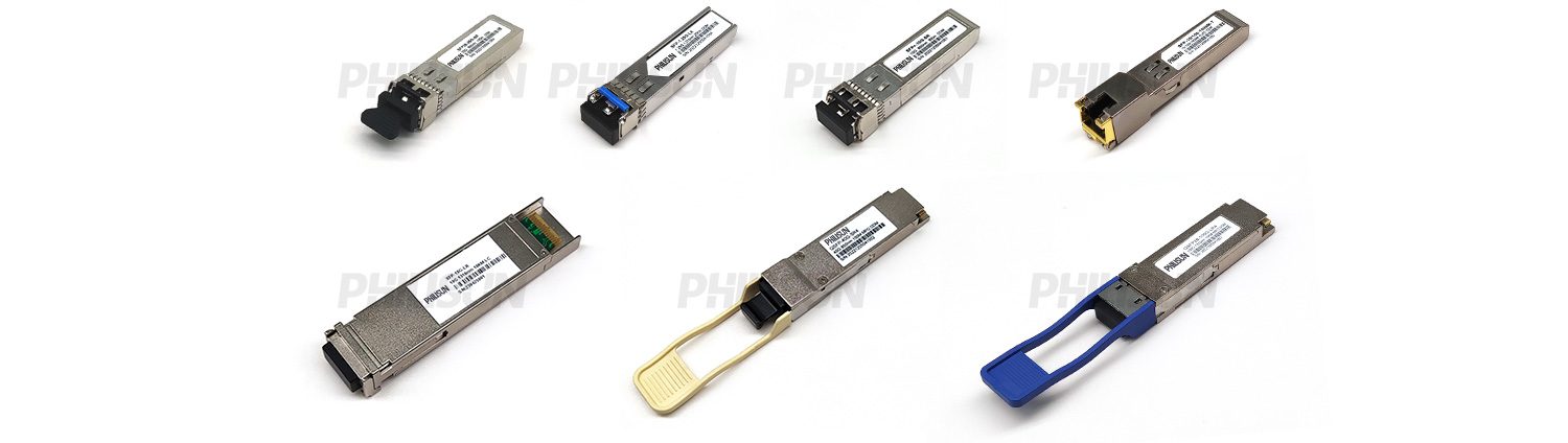
TRANSCEIVER SERIES PRODUCTS
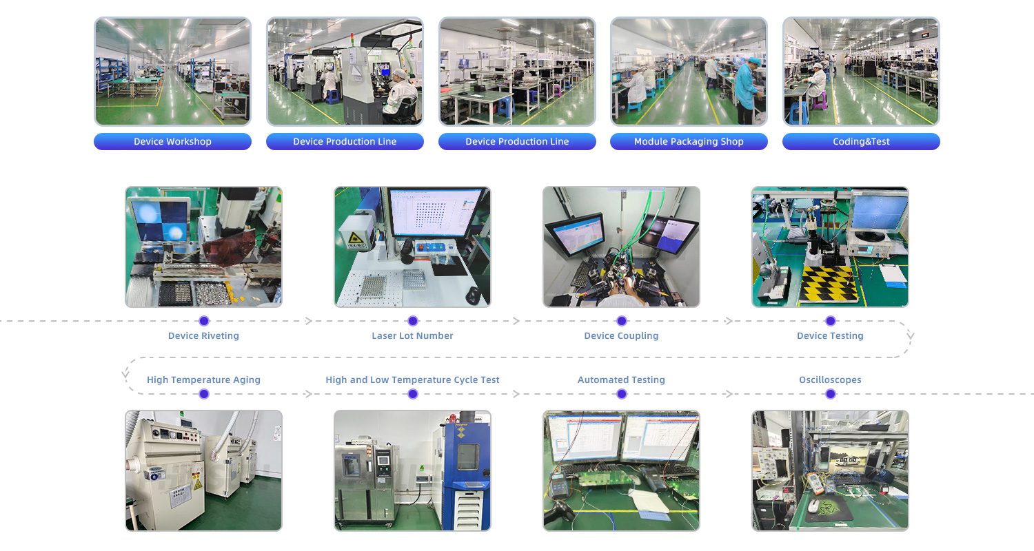
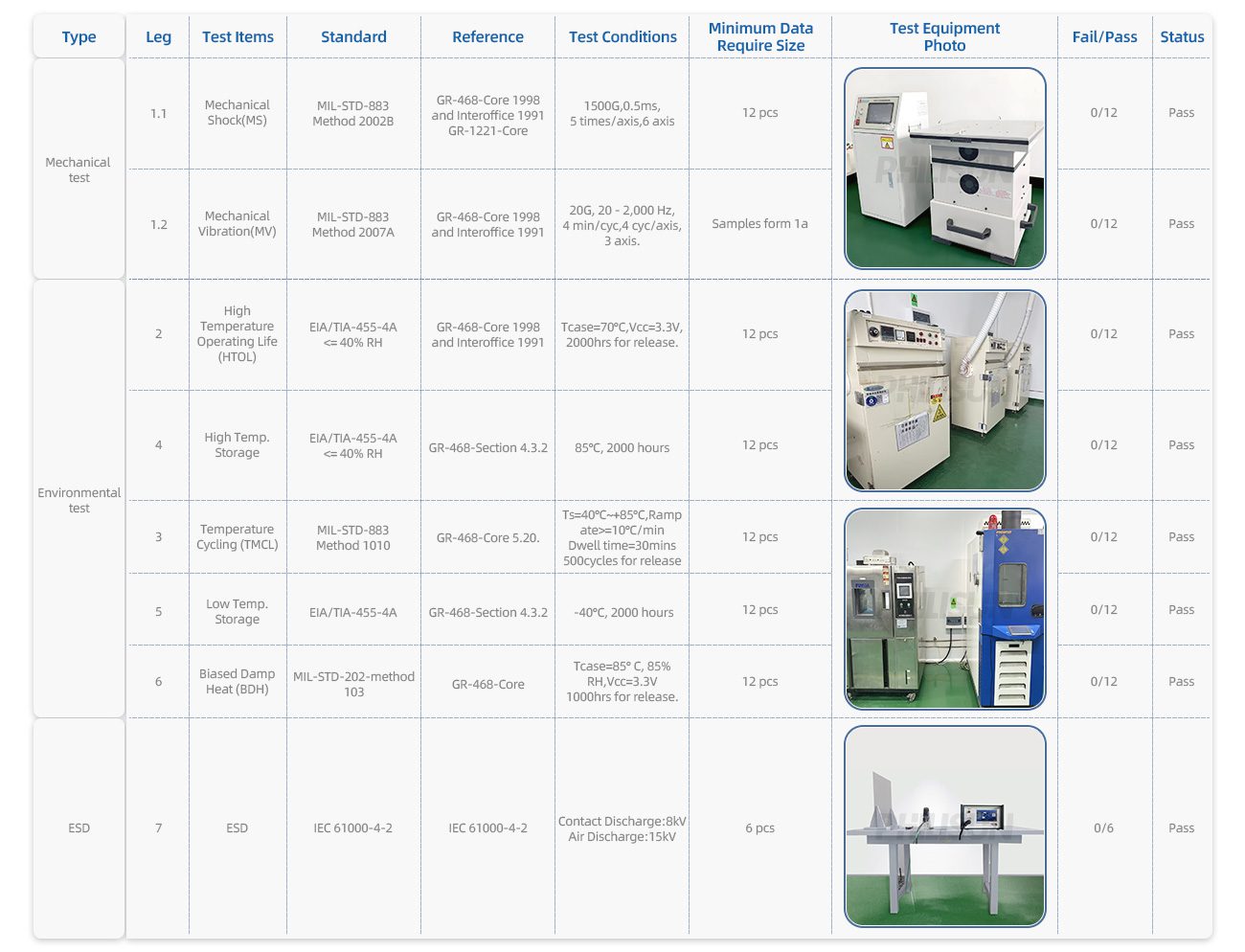
PRODUCTION & TESTING EQUIPMENT
PERFORMANCE PARAMETER
| Absolute Maximum Ratings | |||||||||
| Parameter | Symbol | Min. | Max. | Unit | |||||
| Supply voltage | Vcc | -0.3 | +4.0 | V | |||||
| Storage temperature | Ts | -40 | +85 | ℃ | |||||
| Operating humidity | RH | 0 | +85 | % | |||||
| General Specifications | |||||||||
| Parameter | Symbol | Min | Typ. | Max | Unit | ||||
| Bit rate | BR | – | 25.78 | – | Gbps | ||||
| Bit Error ratio | BER | – | – | 5*10E-5 | – | ||||
| Max. supported link length | Lmax | – | – | 100 | m | ||||
| Recommended Operating Conditions | |||||||||
| Parameter | Symbol | Min. | Typ. | Max. | Unit | ||||
| Operating temperature | Tc | 0 | – | +70 | °C | ||||
| Power supply voltage | Vcc | 3.1 | 3.3 | 3.46 | V | ||||
| Bit rate | BR | – | 25.78 | – | Gbps | ||||
| Max. supported link length | LMAX | – | – | 100 | m | ||||
| Electrical Characteristics | |||||||||
| Parameter | Symbol | Min. | Typ. | Max | Unit | Note | |||
| Supply voltage | Vcc | 3.14 | 3.3 | 3.46 | V | – | |||
| Supply current | Icc | – | – | 230 | mA | – | |||
| Transmitter | |||||||||
| Input differential impedance | RIN | 80 | 100 | 120 | Ω | 1 | |||
| Single ended data input swing | VIN | 90 | – | 150 | mVp-p | – | |||
| Transmit disable voltage | VDIS | 2 | – | VCCHOST | V | – | |||
| Transmit enable voltage | VEN | VEE | – | VEE+0.8 | V | – | |||
| Transmit fault assert voltage | VFA | 2 | – | VCCHOST | V | – | |||
| Transmit fault de-assert voltage | VFDA | VEE | – | VEE+0.8 | V | – | |||
| Receiver | |||||||||
| Single ended data output swing | VOD | 200 | – | 500 | mVpp | – | |||
| LOS fault | VLOSFT | 2 | – | VCCHOST | V | – | |||
| LOS normal | VLOSFT | VEE |
–
|
VEE+0.8
|
V | – | |||
| *Notes:Differential between TD+ / TD–. | |||||||||
| Optical Characteristics | |||||||||
| Parameter | Symbol | Min. | Typ. | Max. | Unit | Note | |||
| Transmitter | |||||||||
| Nominal wavelength | λ | 840 | – | 860 | nm | – | |||
| Spectral width | ∆λ | – | – | 0.6 | nm | – | |||
| Optical modulation amplitude | POMA | -6.4 | – | 3 | dBm | – | |||
| Optical output power | POFF | -8.4 | – | 2.4 | dBm | – | |||
| Extinction ratio | ER | 2 | – | – | dB | – | |||
| Transmitter dispersion penalty | TDP | – | – | 5 | dB | – | |||
| Average launch power of OFF Transmitter |
POFF | – | – | -30 | dBm | – | |||
| Receiver | |||||||||
| Center wavelength | λ | 840 | – | 860 | nm | – | |||
| Average receiver power | PAVG | -10.3 | – | 2.4 | dBm | 1 | |||
| Stressed receiver sensitivity(OMA) | RSENSE | – | – | -5.2 | dBm | 2 | |||
| Receiver reflectance | RREFL | – | – | -12 | dB | – | |||
| Assert LOS | LOSA | -30 | – | – | dBm | – | |||
| De-assert LOS | LOSD | – | – | -13 | dBm | – | |||
| LOS hysteresis | 0.5 | dB | – | ||||||
| Notes: 1. Sensitivity for 25.78G PRBS 231-1 and BER better than or equal to 5*10E-5. 2. The stressed sensitivity values in the table are for system level BER measurements which include the effects of CDR circuit. |
|||||||||
PIN ASSIGNMENT

| Pin Number | Symbol | Name | Description | ||||||
| 1,17,20 | VeeT | Transmitter signal ground | These pins should be connected to signal groundon the host board. | ||||||
| 2 | TX fault | Transmitter fault out (OC) | Logic “1” output = Transmitter fault Logic “0” output = Normal operation This pin is open collector compatible, and should be pulled up to host Vcc with a 10kΩ resistor. |
||||||
| 3 | TX disable | Transmitter disable in (LVTTL) | Logic “1” input (or no connection) = Laser off Logic “0” Input = Laser on This pin is internally pulled up to VccT with a 10 kΩ resistor |
||||||
| 4 | SDA | Module definition identifiers | Serial ID with SFF 8472 diagnostics module definition pins should be pulled up to Host Vcc with 10 kΩ resistors. | ||||||
| 5 | SCL | ||||||||
| 6 | MOD-ABS | ||||||||
| 7 | RS0 | Receiver rate select (LVTTL) Transmitter rate select (LVTTL) |
NA | ||||||
| 9 | RS1 | NA | |||||||
| 8 | LOS | Loss of signal out (OC) | This pin is open collector compatible, and should be pulled up to host Vcc with a 10kΩ resist |
||||||
| 10,11,14 | VeeR | Receiver signal ground | These pins should be connected to signal groundon the host board. | ||||||
| 12 | RD- | Receiver negative DATA out (CML) | Light on = logic “0” output receiver DATA output is internally AC coupled and series terminated with a 50Ω resistor. | ||||||
| 13 | RD+ | Receiver positive DATA out(CML) | Light on = Logic “1” output receiver DATA output is internal ly AC coupled and series terminated with a 50 Ω resistor. |
||||||
| 15 | VccR | Receiver power supply | This pin should be connected to a filtered +3.3V power supply on the host board. See figure 3.recommended power supply filter | ||||||
| 16 | VccT | Transmitter power supply | This pin should be connected to a filtered +3.3V power supply on the host board. See figure 3.recommended power supply filter | ||||||
| 18 | TD+ |
Transmitter positive DATA in(CML)
|
Logic “1” input = light on transmitter DATA inputs are internally AC coupled and terminated with a differential 100Ω resistor. | ||||||
| 19 | TD- | Transmitter negative DATA in(CML) | Logic “0” input = light on transmitter DATA inputs are internally AC coupled and terminated with a differential 100Ω resistor. | ||||||
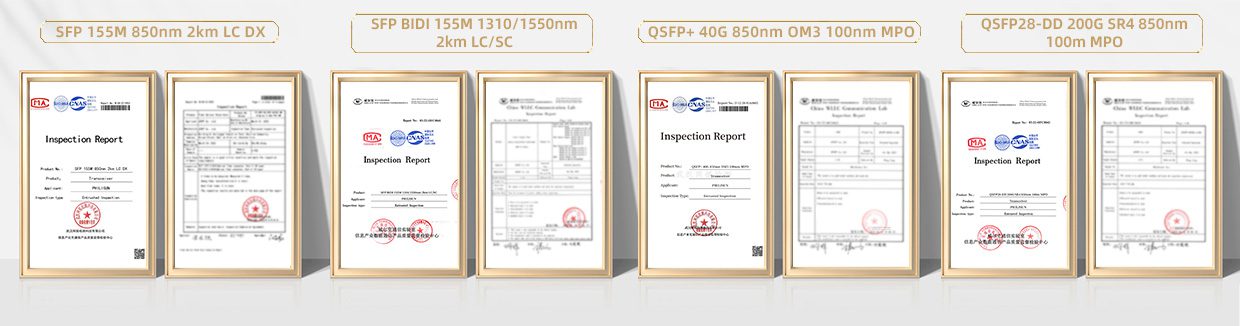
PRODUCT CERTIFICATION
QUALITY ADVANTAGE
COMPATIBLE BRANDS

CONFIGURATION INFORMATION
Related products
-
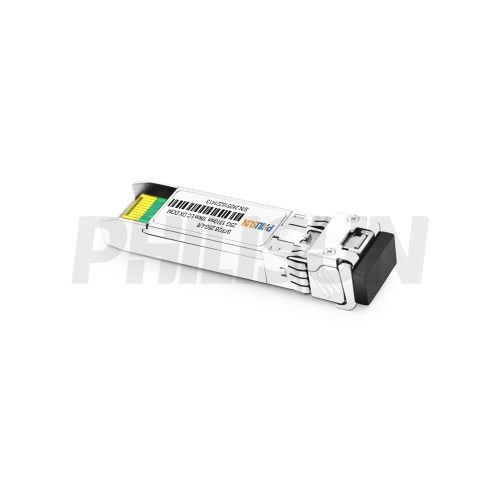
25GBASE-LR SFP28 1310nm 10km DOM Duplex LC SMF Transceiver
SFP28-25-13-10(LR)-LCD
-
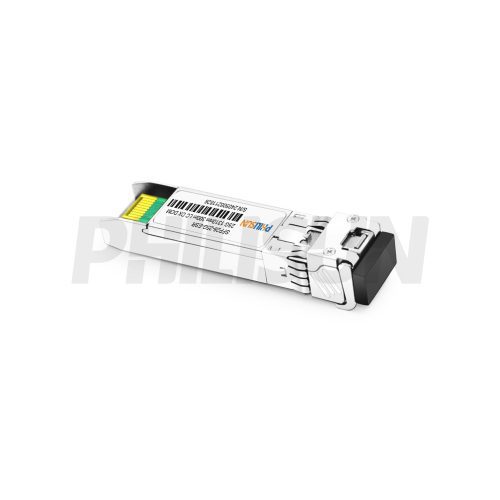
Generic Compatible 25G ESR SFP28 1310nm 300m DOM Duplex LC MMF Optical Transceiver Module
SFP28-25-13-03(ESR)-LCD
-
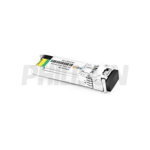
Generic Compatible 25G LRL SFP28 1310nm 2km DOM Duplex LC SMF Optical Transceiver Module
SFP28-25-13-2(LRL)-LCD
-
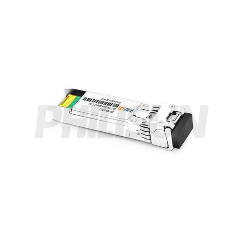
Generic Compatible 25G ER SFP28 1310nm 30km DOM Duplex LC SMF Optical Transceiver Module
SFP28-25-13-30(ER)-LCD