

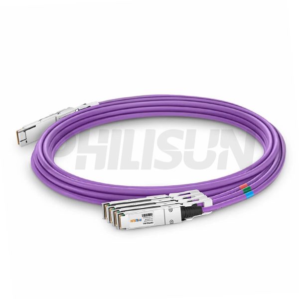
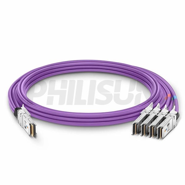
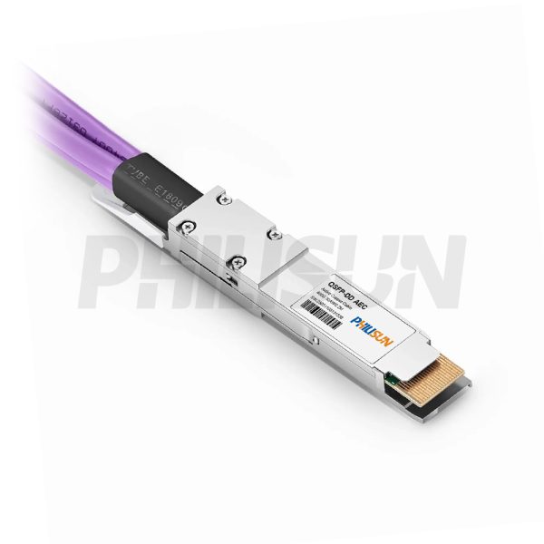
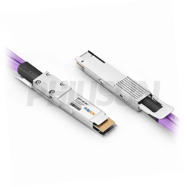
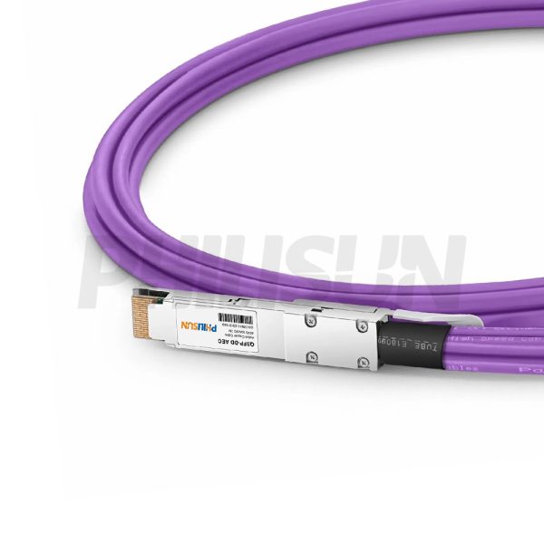
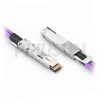

400G QSFP-DD to 4×100G QSFP28 AEC
Compliant with
QSFP-DD MSA、SFF-8636 standard
Switch to Switch
Switch to GPU
- High Quality
- Factory Outlet
- Satisfaction Guarantee
- Global Shipping
| SPECIFICATIONS | |||
|---|---|---|---|
| Cable End Connector A | QSFP-DD | Cable End Connector B | 4×QSFP28 |
| Jumper Type | Direct-Attach Breakout | Data Rate | 400G |
| Aggregate Bit Rate | 425Gbps | Lane Bit Rate | QSFP-DD:53.125Gbps QSFP28:25.78125Gbps |
| Number of Channels | QSFP-DD:8 TX and 8 RX per Module (PAM4) QSFP28:4 TX and 4 RX per Module (NRZ) | Single Channel Rate | QSFP-DD:53.125Gb/s; 25.78125Gb/s QSFP28: 25.78125Gb/s |
| Minimum Bend Radius | 5X Cable OD | Factory Brand | PHILISUN |
| Management Interface | I²c | Bit Error Rate | ≤10-12 |
| Shield | Braid/Foil | Wire AWG | 30AWG |
| Cable Type | Active Twinax | Cable OD | 30AWG: 5.3mm |
| Cable Colour/Material | Black PVC(OFNR) | Cable Length Selection | 1-5 meter |
| Protocols | QSFP-DD MSA/SFF-8679/SFF-8636 | Application Scenarios | 400 Gigabit Ethernet (400GbE) |
| Supply Voltage | 3.3V | Power Dissipation | QSFP-DD:≤8.5W QSFP28:≤3.5W |
| Operating Temperature | 0 to 70℃ (32 to 158℉) | Storage Temperature | -40 to 85℃ (-40 to 185℉) |
PRODUCT PRESENTATION
The PHILISUN 400G QSFP-DD to 4x100G QSFP28 Active Electrical Copper Breakout Cable is a crucial tool for high-density network migration and port utilization. It efficiently links a single 400G QSFP-DD switch port (using 53.125Gbps PAM4 lanes) to four downstream 100G QSFP28 server ports (using 25.78125Gbps NRZ lanes). Featured with low latency and reliable performance, this cable enables massive breakout connectivity vital for scaling capacity in data center fabrics and supporting the growing demand for 100G server-to-ToR links.
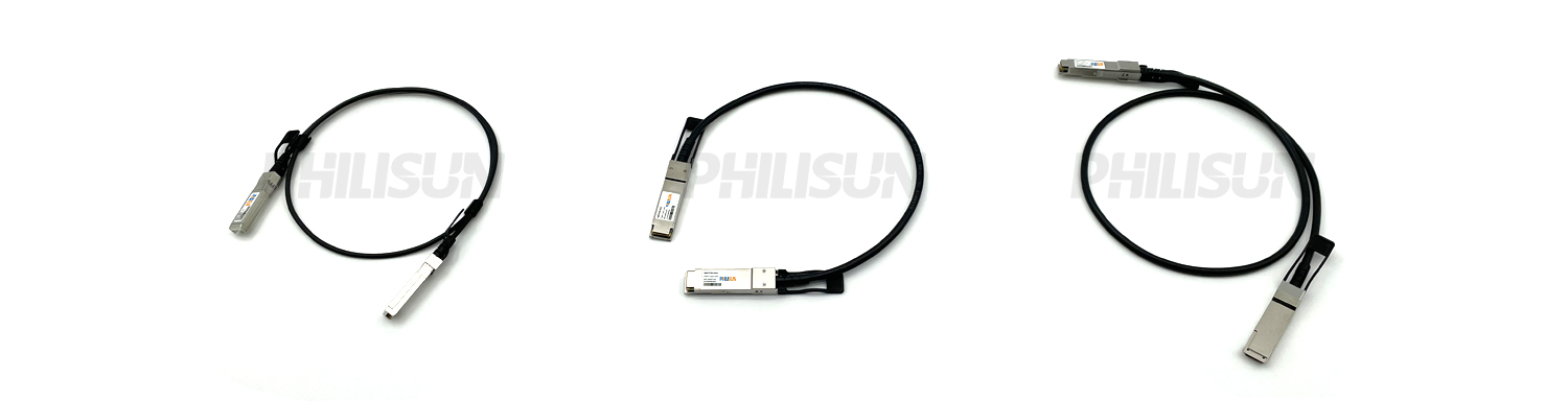
AEC SERIES PRODUCTS
PRODUCTION & TESTING EQUIPMENT

PERFORMANCE PARAMETER
| Absolute Maximum Ratings | |||||||||
| Parameter | Min. | Max. | Unit | ||||||
| Supply Voltage | -0.3 | 3.465 | V | ||||||
| Data Input Voltage | 0 | 1.8 | V | ||||||
| Control Input Voltage | -0.3 | 3.6 | V | ||||||
| Storage Temperature Range | – 10 | +85 | °C | ||||||
| Operating Case Temperature Range | 0 | +70 | °C | ||||||
| Operating Relative Humidity | 0 | 80 | % | ||||||
| General Product Characteristics | |||||||||
| Parameter | Value | Comments | |||||||
| Module Form Factor | QSFP- DD and QSFP28 | – | |||||||
| N umber of Data Lanes | 8 TX and 8 RX per Module (PAM4) | QSFP- DD | |||||||
| 4 TX and 4 RX per Module (NRZ) | QSFP28 | ||||||||
| Maximum Aggregate Data Rate | 400Gbps | – | |||||||
| Nominal Data Rate per Lane | 53. 125Gbps (PAM4) | QSFP- DD | |||||||
| 25.78125Gbps (NRZ) | QSFP28 | ||||||||
| Electrical I nterface and Pin-out | 76- Pinedge Connector | QSFP- DD | |||||||
| 38- Pinedge Connector | QSFP28 | ||||||||
| Pin Description | Per QSFP- DD Hardware Specification (QSFP- DD) and per SFF-8679 (QSFP28) |
– | |||||||
| Management Interface | I2C, Serial, Timing per Common Management Interface Specification for 8X/ 16X Pluggable Transceivers |
QSFP-DD | |||||||
| I2C, Serial, Timing per SFF-8636 | QSFP28 | ||||||||
| Length of AEC | 1, 3, 5 | Meters, Using Copper | |||||||
| BER ( P re- FEC) | < 10-8 | Tested with QPRBS31 Pattern | |||||||
| BER ( Post- FEC) | < 10-15 | Tested with QPRBS31 Pattern | |||||||
| Power Supply (DC) | 3.3V | – | |||||||
| Electrical Specifications | |||||||||
| Parameter | Conditions | Min. | Typ. | Max. | Units | ||||
| Power Consumption @QSFP- DD | – | – | 8.5 | – | W | ||||
| Power Consumption @QSFP28 | – | – | 3.5 | – | W | ||||
| Supply Voltage, VccTx, VccRx | – | 3.135 | 3.3 | 3.465 | VDC | ||||
| Supply Current, Icc@QSFP- DD | – | – | 2570 | – | mA | ||||
| Supply Current, Icc@QSFP28 | – | – | 1050 | – | mA | ||||
| Power Supply Noise Tolerance | – | – | 25 | – | mVpp | ||||
| Active Cable Input Electrical Characteristics per Lane | |||||||||
| Input Differential Voltage | – | – | Complies with Standards | – | – | ||||
| Signaling Rate/Channel @QSFP- DD | PAM4 | – | 53.125 25.78125 |
– | Gb/s | ||||
| Signaling Rate/Channel @QSFP28 | NRZ | – | 25.78125 | – | Gb/s | ||||
| RX Input Resistance | – | 90 | 100 | ohms | 110 | ||||
| Input Jitter Tolerance | – | – | Complies with Standards | – | – | ||||
| Input Common Mode Noise | – | – | – | 10 | mV- rms | ||||
| ESD Ratings | |||||||||
| ESD Standard | Level | Maximum Rating | Units | ||||||
| Contact Discharge | Air Discharge | ||||||||
| IEC/EN6100-4-2 | 4 | ±8k | ±15k | V | |||||
| Parameter | Conditions | Min. | Typ. | Max. | Units | ||||
| Active Cable Output Electrical Characteristics per Lane | |||||||||
| Output Equalization Coefficient Step Size | – | 1.5 | – | 5 | % | ||||
| Output Total Jitter | Complies with standards | ||||||||
| TX Output Impedance | 80 | 100 | 120 | ohms | |||||
| Latency Characteristics | |||||||||
| Total Latency | – | – | – | 160 | ns | ||||
| Module Output Characteristics (atTP4*)-QSFP-DD End | |||||||||
| Notes: *Please refer to IEEE802.3bs 120E and IEEE802.3bm 83E for TP4 definition. | |||||||||
| Parameter | Value | Units | |||||||
| Signaling Rate Per Lne (Range) | 26.5625± 100 ppm | GBd | |||||||
| AC Common-mode Output Voltage (Max, RMS) | 17.5 | mV | |||||||
| Differential Peak-to- Peak Output Voltage (Max.) | 900 | mV | |||||||
| Near-End ESMW (Eye Symmetry Mask Width) | 0.265 | UI | |||||||
| Near-End Eye Height, Differential (Min.) | 70 | mV | |||||||
| Far-End ESMW (Eye Symmetry Mask Width) | 0.2 | UI | |||||||
| Far-End Eye Height, Differential (Min.) | 30 | mV | |||||||
| Transition Time (Min. 20% to 80%) | 9.5 | ps | |||||||
| DC Common Mode Voltage (Min.)a | –350 | mV | |||||||
| DC Common Mode Voltage (Max.)a | 2850 | mV | |||||||
| Module Output Characteristics (atTP4*)-QSFP28 End | |||||||||
| Notes: *Please refer to IEEE802.3bs 120E and IEEE802.3bm 83E for TP4 definition. | |||||||||
| Parameter | Value | Units | |||||||
| Signaling Rate per Lane (Range) | 25.78125± 100ppm | GBd | |||||||
| AC Common-Mode Output Voltage (Max, RMS) | 17.5 | mV | |||||||
| Differential Output Voltage (Max.) | 900 | mV | |||||||
| Eyewidth (Min.) | 0.57 | UI | |||||||
| Eyeheight, Differential (Min.) | 228 | mV | |||||||
| Transition Time (Min. 20% to 80%) | 12 | ps | |||||||
| DC Common Mode Voltage (Min.)a | –350 | mV | |||||||
| DC Common Mode Voltage (Max.)a | 2850 | mV | |||||||
| A DC common mode voltage is generated by the host. Specification includes effects of ground offset voltage. | |||||||||
Pin Description-QSFP28 End
QSFP-DD MSA-compliant 76-pin Connector
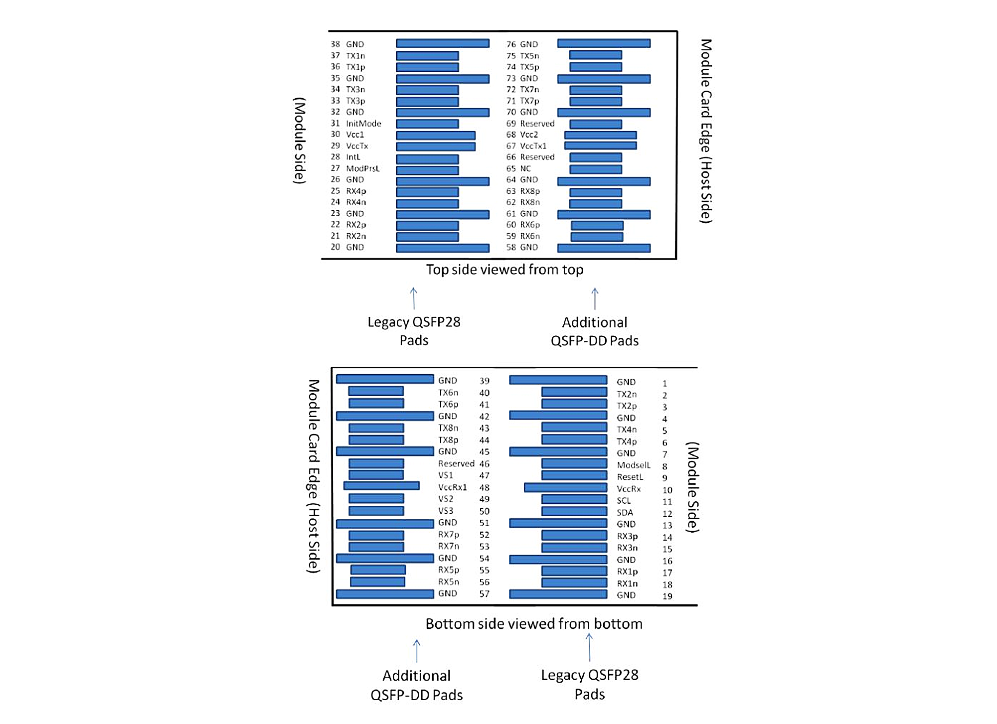
| Pin | Symbol | Description | |||||||
| 1 | GND | Ground | |||||||
| 2 | Tx2n | Transmitter Inverted Data Input | |||||||
| 3 | Tx2p | Transmitter Non-Inverted Data Input | |||||||
| 4 | GND | Ground | |||||||
| 5 | Tx4n | Transmitter Inverted Data Input | |||||||
| 6 | Tx4p | Transmitter Non-Inverted Data Input | |||||||
| 7 | GND | Ground | |||||||
| 8 | ModSelL | Module Select | |||||||
| 9 | ResetL | Module Reset | |||||||
| 10 | VccRx | +3.3V Power Supply Receiver | |||||||
| 11 | SCL | 2-wireserial Interface Clock | |||||||
| 12 | SDA | 2-wireserial Interface Data | |||||||
| 13 | GND | Ground | |||||||
| 14 | Rx3p | Receiver Non-Inverted Data Output | |||||||
| 15 | Rx3n | Receiver Inverted Data Output | |||||||
| 16 | GND | Ground | |||||||
| 17 | Rx1p | Receiver Non-Inverted Data Output | |||||||
| 18 | Rx1n | Receiver Inverted Data Output | |||||||
| 19 | GND | Ground | |||||||
| 20 | GND | Ground | |||||||
| 21 | Rx2n | Receiver Inverted Data Output | |||||||
| 22 | Rx2p | Receiver Non-Inverted Data Output | |||||||
| 23 | GND | Ground | |||||||
| 24 | Rx4n | Receiver Inverted Data Output | |||||||
| 25 | Rx4p | Receiver Non-Inverted Data Output | |||||||
| 26 | GND | Ground | |||||||
| 27 | ModPrsL | Module Present | |||||||
| 27 | ModPrsL | Module Present | |||||||
| 28 | IntL | Interrupt | |||||||
| 29 | VccTx | +3.3V Power Supply Transmitter | |||||||
| 30 | Vcc 1 | +3.3VPower Supply | |||||||
| 31 | InitMode | Initialization mode; In legacy QSFP applications, the InitMode pad is called LPMODE |
|||||||
| 32 | GND | Ground | |||||||
| 33 | Tx3p | Transmitter Non-Inverted Data Input | |||||||
| 34 | Tx3n | Transmitter Inverted DataInput | |||||||
| 35 | GND | Ground | |||||||
| 36 | Tx1p | Transmitter Non-Inverted Data Input | |||||||
| 37 | Tx1n | Transmitter Inverted Data Input | |||||||
| 38 | GND | Ground | |||||||
| 39 | GND | Ground | |||||||
| 40 | Tx6n | Transmitter Inverted Data Input | |||||||
| 41 | Tx6p | Transmitter Non-Inverted Data Input | |||||||
| 42 | GND | Ground | |||||||
| 43 | Tx4n | Transmitter Inverted Data Input | |||||||
| 44 | Tx4p | Transmitter Non-Inverted Data Input | |||||||
| 45 | GND | Ground | |||||||
| 46 | Reserved | For Future Use | |||||||
| 47 | VS1 | Module Vendor Specific 1 | |||||||
| 48 | VccRx1 | 3.3V Power Supply | |||||||
| 49 | VS2 | Module Vendor Specific 2 | |||||||
| 50 | VS3 | Module Vendor Specific 3 | |||||||
| 51 | GND | Ground | |||||||
| 52 | Rx7p | Receiver Non-Inverted Data Output | |||||||
| 53 | Rx7n | Receiver Inverted Data Output | |||||||
| 54 | GND | Ground | |||||||
| 55 | Rx5p | Receiver Non-Inverted Data Output | |||||||
| 56 | Rx5n | Receiver Inverted Data Output | |||||||
| 57 | GND | Ground | |||||||
| 58 | GND | Ground | |||||||
| 59 | Rx6n | Receiver Inverted Data Output | |||||||
| 60 | Rx6p | Receiver Non-Inverted Data Output | |||||||
| 61 | GND | Ground | |||||||
| 62 | Rx8n | Receiver Inverted Data Output | |||||||
| 67 | VccT 1x | 3.3V Power Supply | |||||||
| 68 | Vcc2 | 3.3V Power Supply | |||||||
| 69 | Reserved | For Future Use | |||||||
| 70 | GND | Ground | |||||||
| 71 | Tx7p | Transmitter Non-Inverted Data Input | |||||||
| 72 | Tx7n | Transmitter Inverted Data Input | |||||||
| 73 | GND | Ground | |||||||
| 74 | Tx5p | Transmitter Non-Inverted Data Input | |||||||
| 75 | Tx5n | Transmitter Inverted Data Input | |||||||
| 76 | GND | Ground | |||||||
Pin Description-QSFP28 End
QSFP-compliant 38-pin Connector (per SFF-8679)
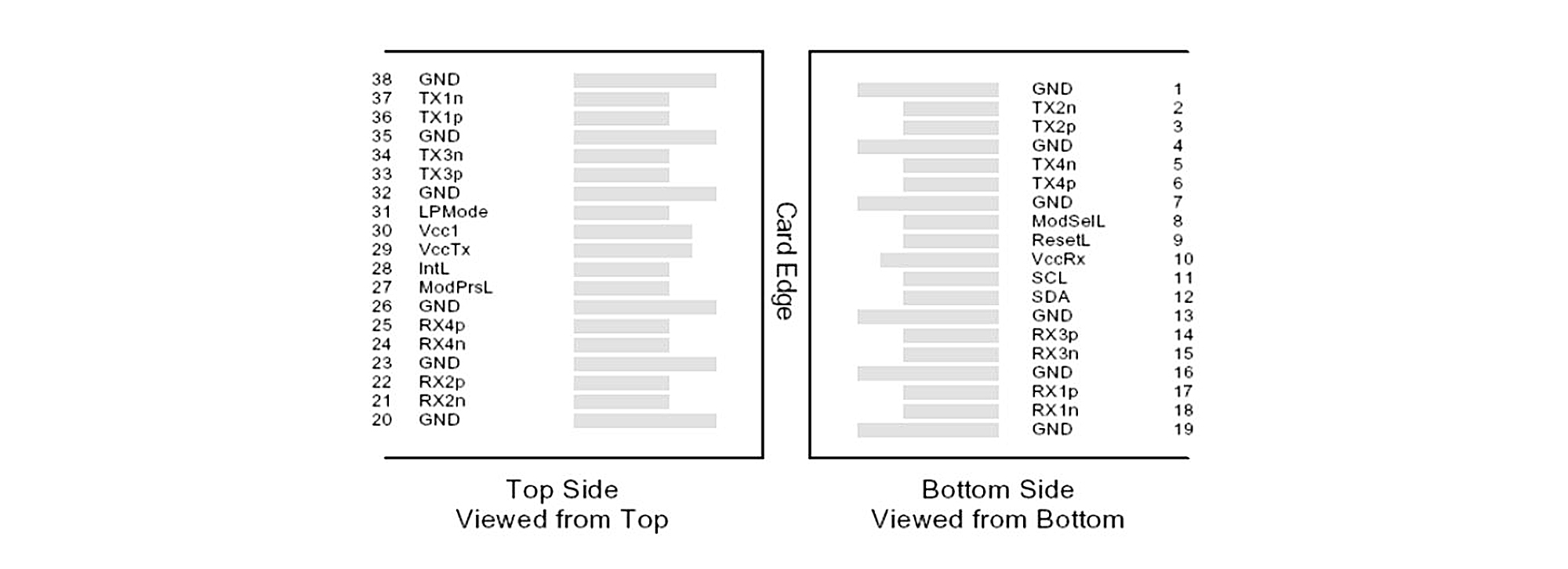
| Pin | Symbol | Description | |||||||
| 1 | GND | Ground | |||||||
| 2 | Tx2n | Transmitter Inverted Data Input | |||||||
| 3 | Tx2p | Transmitter Non-Inverted Data Input | |||||||
| 4 | GND | Ground | |||||||
| 5 | Tx4n | Transmitter Inverted Data Input | |||||||
| 6 | Tx4p | Transmitter Non-Inverted Data Input | |||||||
| 7 | GND | Ground | |||||||
| 8 | ModSelL | Module Select | |||||||
| 9 | ResetL | Module Reset | |||||||
| 10 | VccRx | +3.3V Power Supply Receiver | |||||||
| 11 | SCL | 2-Wireserial Interface Clock | |||||||
| 12 | SDA | 2-Wireserial Interface Data | |||||||
| 13 | GND | Ground | |||||||
| 14 | Rx3p | Receiver Non-Inverted Data Output | |||||||
| 15 | Rx3n | Receiver Inverted Data Output | |||||||
| 16 | GND | Ground | |||||||
| 17 | Rx1p | Receiver Non-Inverted Data Output | |||||||
| 18 | Rx1n | Receiver Inverted Data Output | |||||||
| 19 | GND | Ground | |||||||
| 20 | GND | Ground | |||||||
| 21 | Rx2n | Receiver Inverted Data Output | |||||||
| 22 | Rx2p | Receiver Non-Inverted Data Output | |||||||
| 23 | GND | Ground | |||||||
| 24 | Rx4n | Receiver Inverted Data Output | |||||||
| 25 | Rx4p | Receiver Non-Inverted Data Output | |||||||
| 26 | GND | Ground | |||||||
| 27 | ModPrsL | Module Present | |||||||
| 28 | IntL | Interrupt | |||||||
| 29 | VccTx | +3.3V Power Supply Transmitter | |||||||
| 30 | Vcc1 | +3.3V Power Supply | |||||||
| 31 | LPMode | Low Power Mode | |||||||
| 32 | GND | Ground | |||||||
| 33 | Tx3p | Transmitter Non-Inverted Data Input | |||||||
| 34 | Tx3n | Transmitter Inverted Data Input | |||||||
| 35 | GND | Ground | |||||||
| 36 | Tx1p | Transmitter Non-Inverted Data Input | |||||||
| 37 | Tx1n | Transmitter Inverted Data Input | |||||||
| 38 | GND | Ground | |||||||
| Cable Mechanical Specifications | |||||||||
| Parameter | Types | Min. | Typ. | Max. | Units | ||||
| Diameter | 4P 30AWG | 5.0 | 5.3 | 5.6 | mm | ||||
| QSFP-DD End | |||||||||
| Minimum Bend Radius | 4P 30AWG ×4 | – | 26.5 | – | mm | ||||
| Minimum Bend Space | 4P 30AWG × 4 | – | 73 | mm | |||||
| QSFP28 End | |||||||||
| Minimum Bend Radius | 4P 30AWG | – | 26.5 | – | mm | ||||
| Minimum Bend Space | 4P 30AWG | – | 54 | – | mm | ||||
| Insertion, Extraction and Retention Forces | |||||||||
| Parameter | Min. | Max. | Units | Note | |||||
| Insertion | |||||||||
| QSFP-DD Module | 0 | 90 | N | – | |||||
| QSFP28 Module | 0 | 40 | N | – | |||||
| Extraction | – | – | – | – | |||||
| QSFP-DD Module | 0 | 50 | N | – | |||||
| QSFP28 Module | 0 | 30 | N | – | |||||
| Retention | |||||||||
| QSFP-DD Module | 90 | N/A | N | No Damage to Module Below 90N With Latch Engaged | |||||
| QSFP28 Module | 90 | N/A | N | No Damage to Module Below 90N With Latch Engaged | |||||
| Insertion/Removal Cycles | |||||||||
| QSFP-DD Module | 50 | N/A | Cycles | Number of Cycles for an Individual Module | |||||
| QSFP28 Module | 50 | N/A | Cycles | Number of Cycles for an Individual Module | |||||
| Memory Map QSFP-DD end: Compatible with Common Management Interface Specification for 8X/16X Pluggable Transceivers. QSFP28 end: Compatible with SFF-8636. |
|||||||||
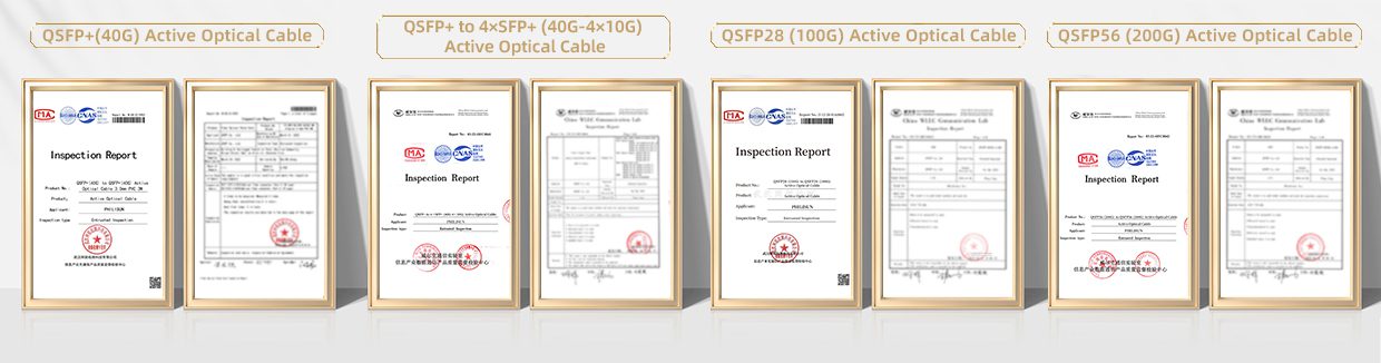
PRODUCT CERTIFICATION
COMPATIBLE BRANDS

CONFIGURATION INFORMATION