

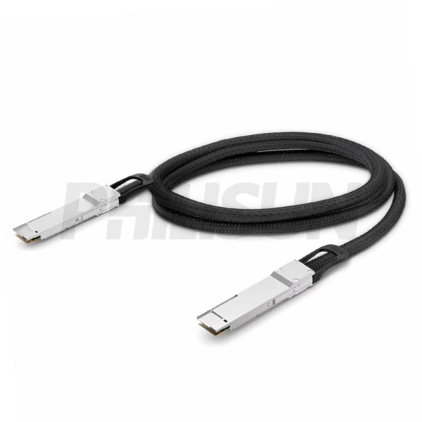
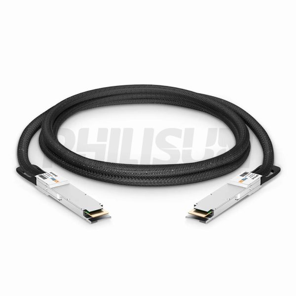
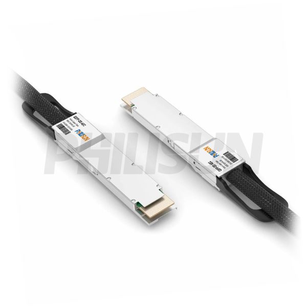
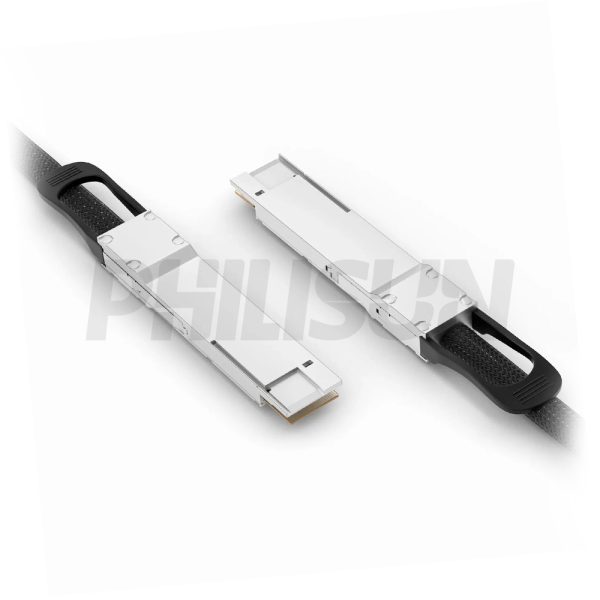
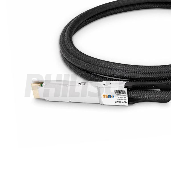
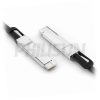
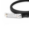
800G QSFP-DD to QSFP-DD Active Electrical Copper Breakout Cable (AEC)
Compliant with
CMIS 5.0,IEEE 802.3ck,QSFP-DD MSA Rev6.3 standard
Switch to Switch
Switch to GPU
- High Quality
- Factory Outlet
- Satisfaction Guarantee
- Global Shipping
| SPECIFICATIONS | |||
|---|---|---|---|
| Cable End Connector A | QSFP-DD | Cable End Connector B | QSFP-DD |
| Jumper Type | Direct-Attach | Data Rate | 800G |
| Aggregate Bit Rate | 850Gbps | Lane Bit Rate | 106.25Gbps |
| Number of Channels | 8 | Single Channel Rate | 100G |
| Minimum Bend Radius | 5X Cable OD | Factory Brand | PHILISUN |
| Management Interface | I²c | Bit Error Rate | ≤10-12 |
| Shield | Braid/Foil | Wire AWG | 28AWG/32AWG |
| Cable Type | Active Twinax | Cable OD | 32AWG: 7.3mm 28AWG: 10.6mm |
| Cable Colour/Material | Purple PET | Cable Length Selection | 1-5 meter |
| Protocols | QSFP-DD MSA/IEEE 802.3ck/CMIS 5.0 | Application Scenarios | 800 Gigabit Ethernet (800GbE) |
| Supply Voltage | 3.3V | Power Dissipation | ≤12.0W |
| Operating Temperature | 0 to 70℃ (32 to 158℉) | Storage Temperature | -40 to 85℃ (-40 to 185℉) |
PRODUCT PRESENTATION
The PHILISUN 800G QSFP-DD AEC (Active Electrical Cable) is a high-speed copper cable with retimer chips on both ends, ensuring signal integrity for 800G Ethernet. It addresses signal loss issues in PAM4 transmission.Compared with passive cables, 800G AEC supports up to 5 meters with low signal attenuation. It provides a QSFP-DD direct-attach solution and complies with QSFP-DD MSA, IEEE 802.3ck and CMIS 5.0. Easy to install, high-speed and cost-effective, it is ideal for short-range connections within or between adjacent racks in data centers.
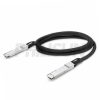
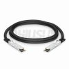
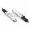
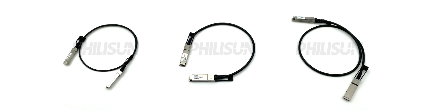
AEC SERIES PRODUCTS
PRODUCTION & TESTING EQUIPMENT

PERFORMANCE PARAMETER
| Absolute Maximum Ratings | |||||||||
| Parameter | Symbol | Min. | Max. | Unit | |||||
| Storage Temperature Range | Ts | – 10 | +85 | ℃ | |||||
| Relative Humidity | RH | 0 | 80 | % | |||||
| Supply Voltage | VCC | -0.3 | 3.465 | V | |||||
| Recommended Operating Conditions | |||||||||
| Parameter | Symbol | Min. | Typ. | Max. | Unit | ||||
| Operating Case Temperature | TOPR | 0 | – | +70 | ℃ | ||||
| Power Supply Voltage | VCC | 3.135 | 3.3 | 3.465 | VDC | ||||
| Bit Rate | BR | – | 800 | – | Gb/s | ||||
| Bit Error Ratio | BER | – | – | <10-15 | – | ||||
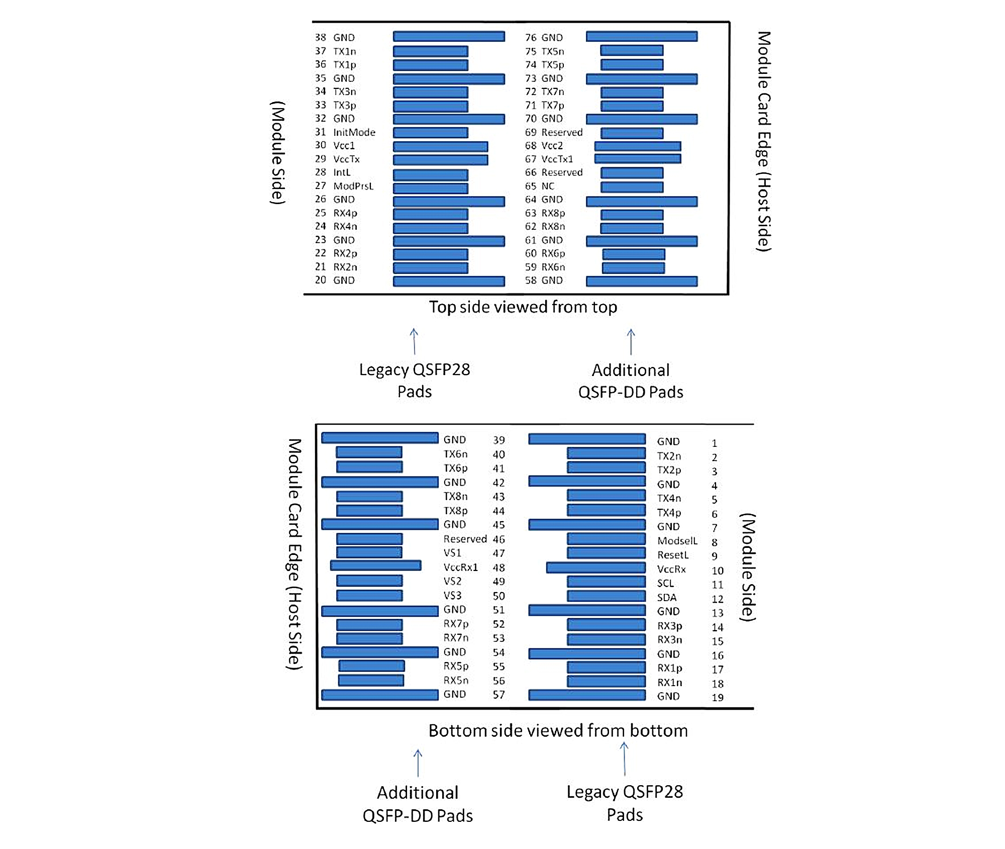
| PIN Definitions for QSFP-DD | |||||||||
| PinNo. | Symbol | Description | |||||||
| 1 | GND | Ground | |||||||
| 2 | Tx2n | Transmitter Inverted Data Input | |||||||
| 3 | Tx2p | Transmitter Non-Inverted Data Input | |||||||
| 4 | GND | Ground | |||||||
| 5 | Tx4n | Transmitter Inverted Data Input | |||||||
| 6 | Tx4p | Transmitter Non-Inverted Data Input | |||||||
| 7 | GND | Ground | |||||||
| 8 | ModSelL | Module Select | |||||||
| 9 | ResetL | Module Reset | |||||||
| 10 | VccRx | +3.3V Power Supply for R | |||||||
| 11 | SCL | 2-Wire Serial Interface Clock | |||||||
| 12 | SDA | 2-Wire Serial Interface Data Line | |||||||
| 13 | GND | Ground | |||||||
| 14 | Rx3p | Receiver Non-Inverted Data Output | |||||||
| 15 | Rx3n | Receiver Inverted Data Output | |||||||
| 16 | GND | Ground | |||||||
| 17 | Rx1p | Receiver Non-Inverted Data Output | |||||||
| 18 | Rx1n | Receiver Inverted Data Output | |||||||
| 19 | GND | Ground | |||||||
| 20 | GND | Ground | |||||||
| 21 | Rx2n | Receiver Inverted Data Output | |||||||
| 22 | Rx2p | Receiver Non-Inverted Data Output | |||||||
| 23 | GND | Ground | |||||||
| 24 | Rx4n | Receiver Inverted Data Output | |||||||
| 25 | Rx4p | Receiver Non-Inverted Data Output | |||||||
| 26 | GND | Ground | |||||||
| 27 | ModPrsL | Module Present | |||||||
| 28 | IntL | Interrupt | |||||||
| 29 | VccTx | +3.3V Power Supply for Transmitter | |||||||
| 30 | Vcc1 | +3.3V Power Supply | |||||||
| 31 | InitMode | Initialization mode; In legacy QSFP applications, the InitMode pad is called LPMODE | |||||||
| 32 | GND | Ground | |||||||
| 33 | Tx3p | Transmitter Non-Inverted Data Input | |||||||
| 34 | Tx3n | Transmitter Inverted Data Input | |||||||
| 35 | GND | Ground | |||||||
| 36 | Tx1p | Transmitter Non-Inverted Data Input | |||||||
| 37 | Tx1n | Transmitter Inverted Data Input | |||||||
| 38 | GND | Ground | |||||||
| 39 | GND | Ground | |||||||
| 40 | Tx6n | Transmitter Inverted Data Input | |||||||
| 41 | Tx6p | Transmitter Non- Inverted Data Input | |||||||
| 42 | GND | Ground | |||||||
| 43 | Tx4n | Transmitter Inverted Data Input | |||||||
| 44 | Tx4p | Transmitter Non- Inverted Data Input | |||||||
| 45 | GND | Ground | |||||||
| 46 | Reserved | For future use | |||||||
| 47 | VSI | Module Vendor Specific 1 | |||||||
| 48 | VccRx1 | 3.3V Power Supply | |||||||
| 49 | VS2 | Module Vendor Specific 2 | |||||||
| 50 | VS3 | Module Vendor Specific 3 | |||||||
| 51 | GND | Ground | |||||||
| 52 | Rx7p | Receiver Non- Inverted Data Output | |||||||
| 53 | Rx7n | Receiver Inverted Data Output | |||||||
| 54 | GND | Module Ground | |||||||
| 55 | Rx5p | Recelver Non- Inverted Data Output | |||||||
| 56 | Rx5n | Recelver Inverted Data Output | |||||||
| 57 | GND | Module Ground | |||||||
| 58 | GND | Module Ground | |||||||
| 59 | Rx6n | Receiver Inverted Data Output | |||||||
| 60 | Rx6p | Recelver Non- Inverted Data Output | |||||||
| 61 | GND | Ground | |||||||
| 62 | Rx8n | Receiver Inverted Data Output | |||||||
| 63 | Rx8p | Receiver Non- Inverted Data Output | |||||||
| 64 | GND | Ground | |||||||
| 65 | NC | No C onnect | |||||||
| 66 | Reserved | For future use | |||||||
| 67 | VccT1x | 3.3V Power Supply | |||||||
| 68 | Vcc2 | 3.3V Power Supply | |||||||
| 69 | Reserved | For future use | |||||||
| 70 | GND | Ground | |||||||
| 71 | Tx7p | Transmitter Non‐Inverted Data Input | |||||||
| 72 | Tx7n | Transmitter Inverted Data Input | |||||||
| 73 | GND | Ground | |||||||
| 74 | Tx5p | Transmitter Non‐Inverted Data Input | |||||||
| 75 | Tx5n | Transmitter Inverted Data Input | |||||||
| 76 | GND | Ground | |||||||
Electrical Pad Layout of QSFP-DD
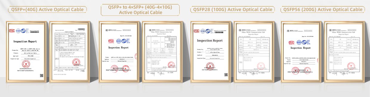
PRODUCT CERTIFICATION
COMPATIBLE BRANDS

CONFIGURATION INFORMATION