

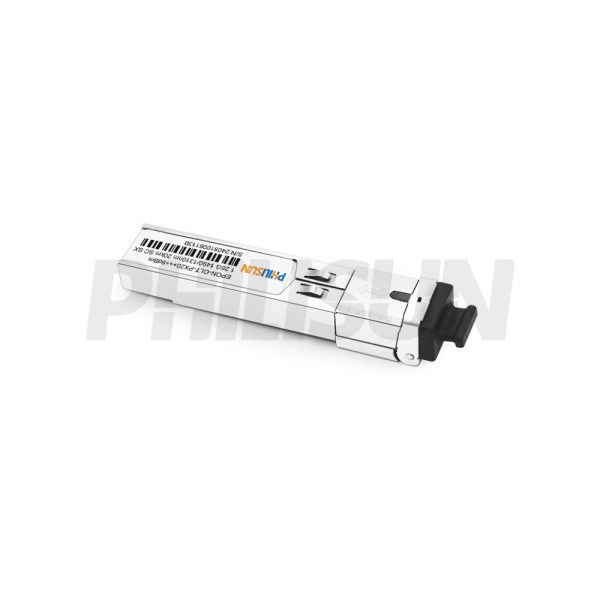
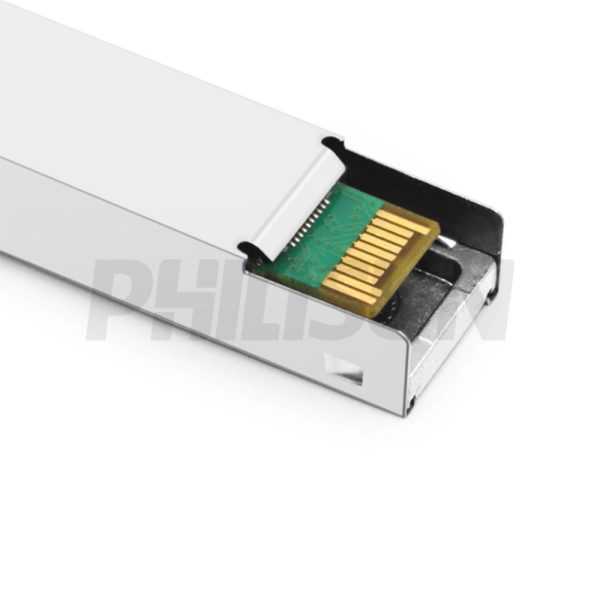
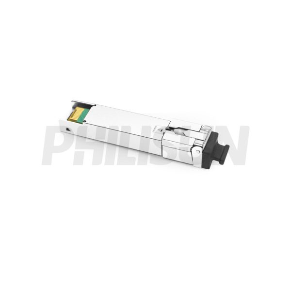
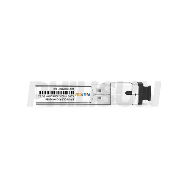
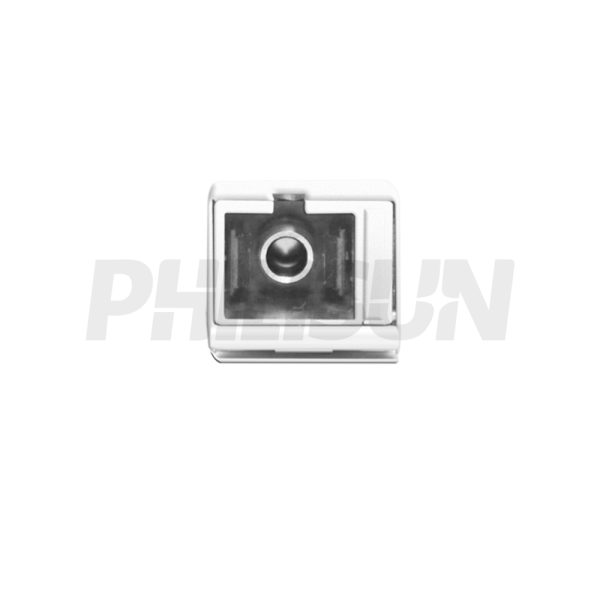
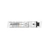
PX20+++ 9dBm EPON OLT 1.25G 20km SC Transceiver
SFP-EPON-PX20+++9dBm-1.25-1413-20-SCS
- High Quality
- Factory Outlet
- Satisfaction Guarantee
- Global Shipping
| SPECIFICATIONS | |||
|---|---|---|---|
| Product Model | SFP-EPON-PX20+++9dBm-1.25-1413-20-SCS | Manufacturer Brand | PHILISUN |
| Package Type | SFP | Optical Connector | SC |
| Max Data Rate | 1.25Gbps | Class | PX20+++ |
| Effective transmission distance | 20KM | ||
| Wavelength | 1310nm/1490nm 1490nm/1310nm | Operating Voltage | 3.3V |
| Fiber Type | SMF | Core Size | 9/125µm |
| Transmitter Type | DFB | Receiver Type | APD |
| TX Power | 8~11dBm | Receiver Sensitivity | -32dBm |
| Digital Diagnostic Monitoring(DDM) | YES | Receiver Overload | -8dBm |
| Power Consumption | <1W | Protocols | SFP MSA SFF-8472 |
| Operating temperature(Commercial) | 0℃~+70℃ | Storage Temperature(Commercial) | -40℃~+85℃ |
| Operating temperature(Industrial) | -40℃~+85℃ | Storage Temperature(Industrial) | -40℃~+85℃ |
PRODUCT PRESENTATION
The PHILISUN EPON OLT PX20+++ 9dBm Transceiver represents the industry-leading 1.25G SFP solution for Optical Line Terminals, enabling 1490nm downstream transmission and 1310nm upstream reception over single-mode fiber (SMF) with 20km reach. Featuring an SC connector and delivering the highest available 9dBm optical budget in the PX20+++ class, this transceiver incorporates 100 Ohm differential impedance on both transmitter inputs and receiver outputs. Its architecture employs internal AC coupling on data lines, provides precision differential termination, and minimizes differential-to-common mode conversion to ensure uncompromising signal integrity, premium termination quality, and ultra-low electromagnetic interference (EMI) performance.
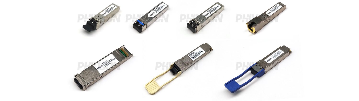
TRANSCEIVER SERIES PRODUCTS
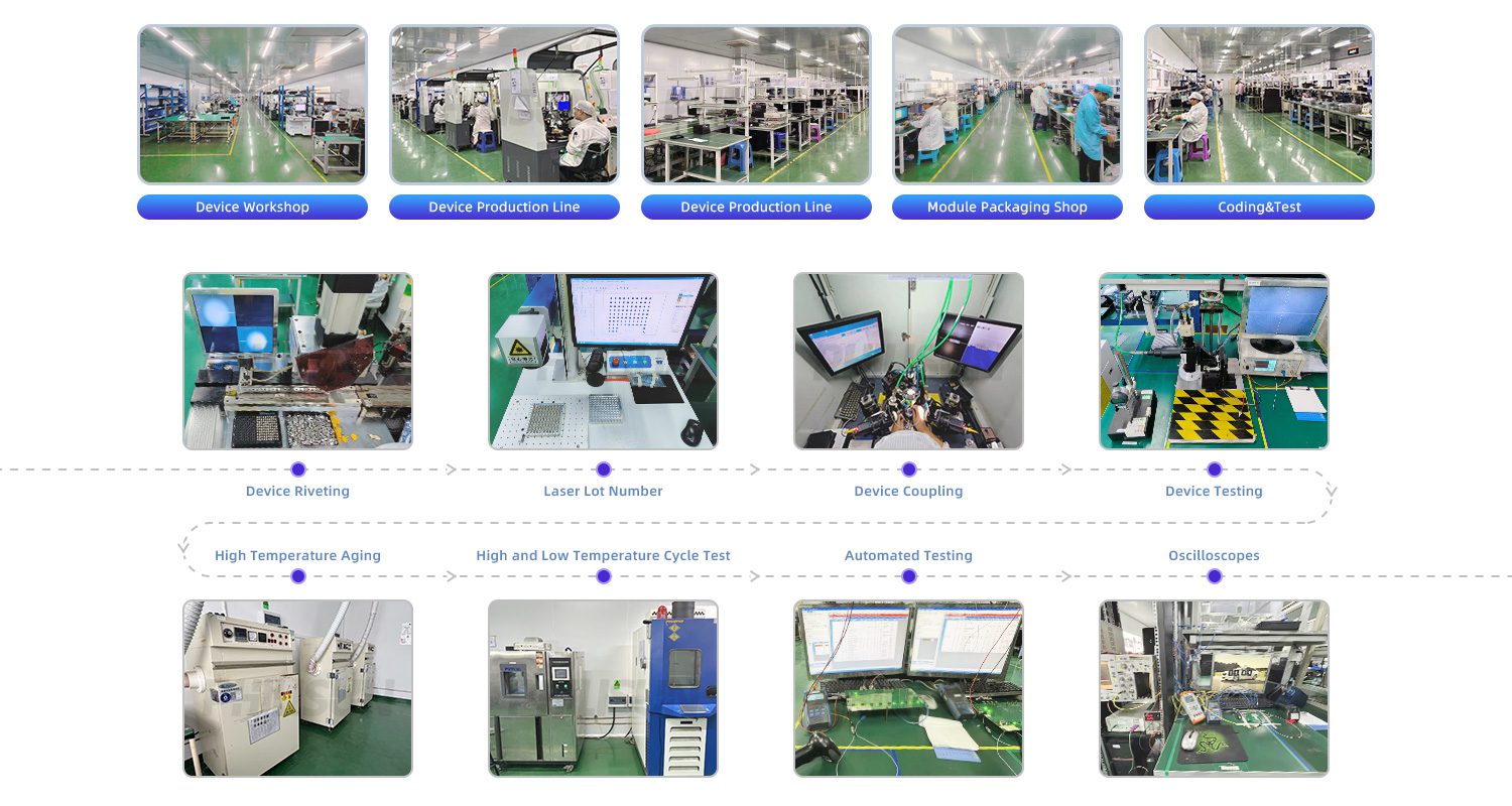
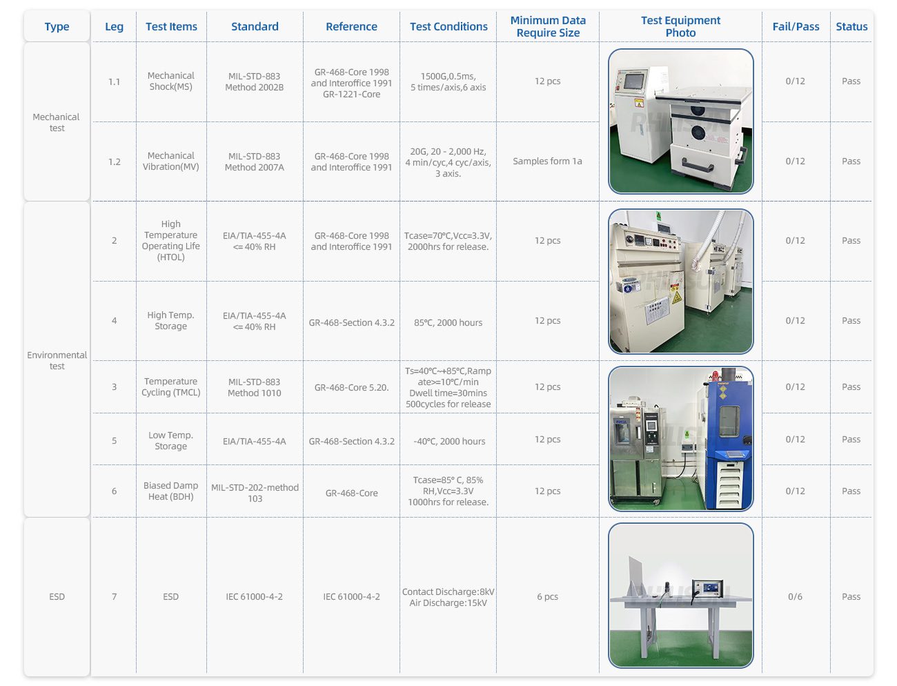
PRODUCTION & TESTING EQUIPMENT
PERFORMANCE PARAMETER
| Absolute Maximum Ratings | |||||||||
| Parameter | Symbol | Min. | Max. | Unit | |||||
| Power Supply Voltage | VCC | 0 | 3.6 | V | |||||
| Storage Temperature | Tc | -40 | 85 | ℃ | |||||
| Operating Case Temperature | Tc | 0 | 70 | ℃ | |||||
| TI | -40 | 85 | |||||||
| Relative Humidity | RH | 5 | 95 | % | |||||
| RX Input Average Power | Pmax | – | -7 | dBm | |||||
| These values represent the damage threshold of the module. Stress in excess of any of the individual Absolute maximum ratings can cause immediate catastrophic damage to the module even if all other parameters are within recommended operating conditions. | |||||||||
| Recommended Operating Environment | |||||||||
| Parameter | Symbol | Min. | Typical | Max. | Unit | ||||
| Power Supply Voltage | VCC | 3.135 | 3.3 | 3.465 | V | ||||
| Power Supply Current | Icc | – | – | 350 | mA | ||||
| Operating Case Temperature |
TC | 0 | 25 | 70 | ℃ | ||||
| TI | -40 | 25 | 85 | ||||||
| Recommended operating environment specifies parameters for which the electrical and optical characteristics hold unless otherwise noted. | |||||||||
| Optical Characteristics | |||||||||
| Parameters | Unit | Values | |||||||
| Operating Reach | m | 2 – 20K | |||||||
| Transmitter | |||||||||
| Center Wavelength | nm | 1490 | |||||||
| Side Mode Suppression Ratio (min) | dB | 30 | |||||||
| Launched power | |||||||||
| – maximum (Average) | dBm | 11 | |||||||
| – typical (Average) | dBm | 9 | |||||||
| – minimum (Average) | dBm | 8 | |||||||
| Average Launch Power of OFF Transmitter (max) | dBm | -30 | |||||||
| Extinction Ratio (min) | dB | 9 | |||||||
| Optical Return Loss Tolerance (min) | dB | 12 | |||||||
| Receiver | |||||||||
| Center Wavelength (range) | nm | 1310 | |||||||
| Receive Overload (max) in Average Power(note 1) | dBm | -8 | |||||||
| Receive Sensitivity (min) in A Power(note 1) | dBm | -32 | |||||||
| Receiver Reflectance (max) | dB | -12 | |||||||
| Los Assert(min) | dBm | -33 | |||||||
| Los Dessert(max) | dBm | -30 | |||||||
| Los Hysteresis(min) | dB | 0.5 | |||||||
| Receiver power (damage, Max) | dBm | -7 | |||||||
| Notes: 1. Average optical power shall be measured using the methods specified in TIA/EIA-455-95. 2. Power budget is defined as the different between the Rx sensitivity andthe Tx output power of the interface. |
|||||||||
| Electrical Characteristics | |||||||||
| Parameter | Symbol | Min. | Typical | Max | Unit | Notes | |||
| Data Rate | – | – | 1.25 | – | Gbps | – | |||
| Power Consumption | – | – | 800 | 1000 | mW | – | |||
| Transmitter | |||||||||
| Single Ended Output Voltage Tolerance | – | -0.3 | – | 4 | V | – | |||
| Common Mode Voltage Tolerance | – | 15 | – | – | mV | – | |||
| Tx Input Diff Voltage | VI | 180 | – | 1200 | mV | – | |||
| Tx Fault | VoL | -0.3 | – | 0.4 | V | At 0.7mA | |||
| Data Dependent Input Jitter | DDJ | – | – | 0.1 | UI | – | |||
| Data Input Total Jitter | TJ | – | – | 0.28 | UI | – | |||
| Receiver | |||||||||
| Single Ended Output Voltage Tolerance | – | -0.3 | – | 4 | V | – | |||
| Rx Output Diff Voltage | Vo | 400 | ‐ | 2400 | mV | LOS Assert Time LOS De‐assert Time | |||
| LOS Assert Time | TAssert | ‐ | ‐ | 500 | ns | ||||
| LOS De‐assert Time | TDeassert | ‐ | ‐ | 500 | ns | ||||
| Receiver Threshold Settling Time | TSETTLING | ‐ | ‐ | 250 | ns | ||||
OLT SFP MODULE PIN DEFINITION
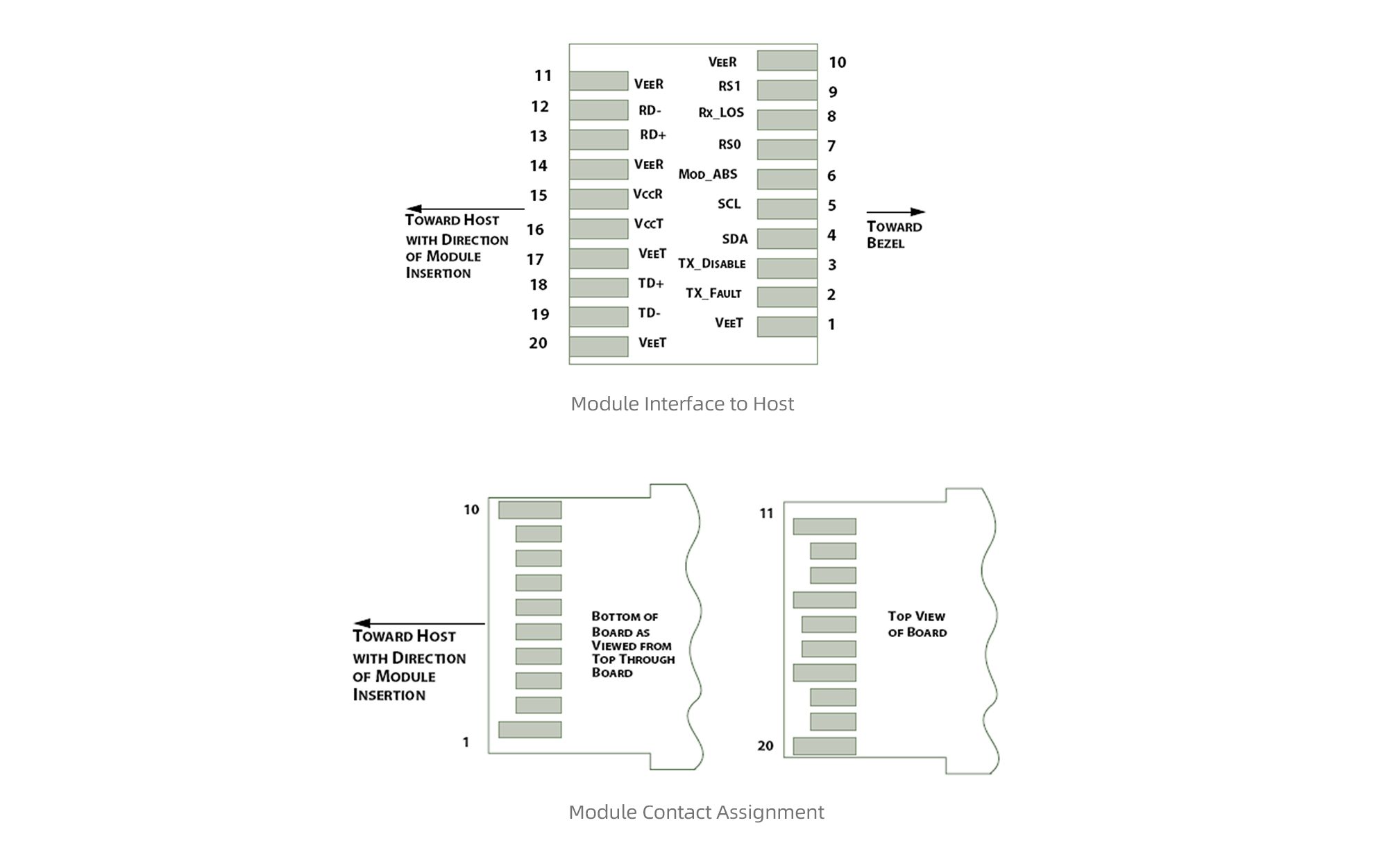
| PIN | Logic | Symbol | Name / Description | Note | |||||
| 1 | – | VeeT | Module Transmitter Ground | 1 | |||||
| 2 | LVTTL-O | TX_Fault | Module Transmitter Fault | – | |||||
| 3 | LVTTL-I | TX_Dis | Transmitter Disable; Turns off Transmitter Laser Output | – | |||||
| 4 | LVTTL-I/O | SDA | 2-Wire Serial Interface Data Line | 2 | |||||
| 5 | LVTTL-I | SCL | 2-Wire Serial Interface Clock | 2 | |||||
| 6 | – | MOD_DEF0 | Module Definition, Grounded in the Module | – | |||||
| 7 | – | NC | Not Connect | – | |||||
| 8 | LVTTL-O | RX_LOS | Receiver Loss of Signal Indication Active LOW | – | |||||
| 9 | – | VeeR | Module Receiver Ground | – | |||||
| 10 | – | VeeR | Module Receiver Ground | 1 | |||||
| 11 | – | VeeR | Module Receiver Ground | 1 | |||||
| 12 | LVPECL-O | RD- | Receiver Inverted Data Output | – | |||||
| 13 | LVPECL-O | RD+ | Receiver Data Output | – | |||||
| 14 | – | VeeR | Module Receiver Ground | 1 | |||||
| 15 | – | VccR |
Module Receiver 3.3 V Supply
|
– | |||||
| 16 | – | VccT | Module Receiver 3.3 V Supply | – | |||||
| 17 | – | VeeT | Module Transmitter Ground | 1 | |||||
| 18 | CML-I | TD+ | Transmitter Non-Inverted Data Input | – | |||||
| 19 | CML-I | TD- | Transmitter Inverted Data Input | – | |||||
| 20 | – | VeeT | Module Transmitter Ground | 1 | |||||
| Note: 1. Module ground pins GND are isolated from the module case. 2. Shall be pulled up with 4.7K-10Kohms to a voltage between 3.15V and 3.45V on the host board. |
|||||||||
PRODUCT CERTIFICATION

QUALITY ADVANTAGE
COMPATIBLE BRANDS

CONFIGURATION INFORMATION
Related products
-
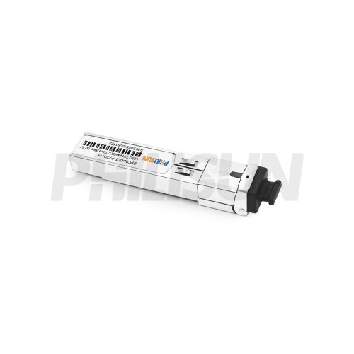
PX20+++ 7dBm EPON OLT 1.25G 1490/1310nm 20km Simplex SC SMF DOM Transceiver
SFP-EPON-PX20+++1.25-1413-20-SCS
-
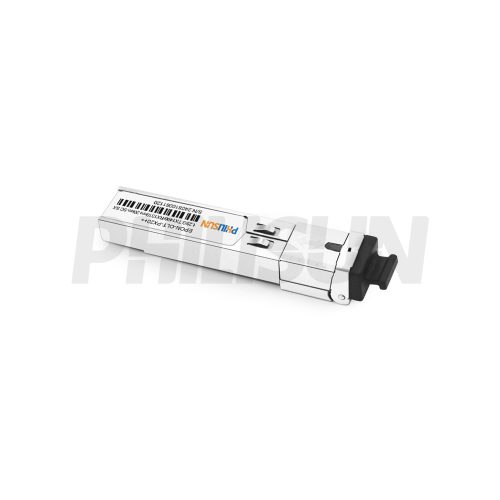
PX20++ 5dBm EPON OLT 1.25G 1490/1310nm 20km Simplex SC SMF DOM Transceiver
SFP-EPON-PX20++1.25-1413-20-SCS
-
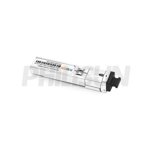
PX20+++ 8dBm EPON OLT 1.25G 1490/1310nm 20km Simplex SC SMF DOM Transceiver
SFP-EPON-PX20+++8dBm-1.25-1413-20-SCS
-
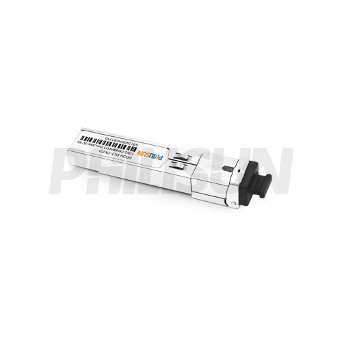
PX20+ 3dBm EPON OLT 1.25G 1490/1310nm 20km Simplex SC SMF DOM Transceiver
SFP-EPON-PX20+1.25-1413-20-SCS