

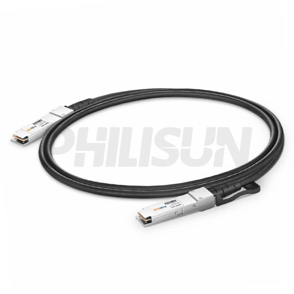
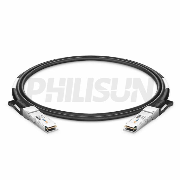
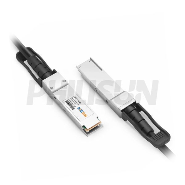
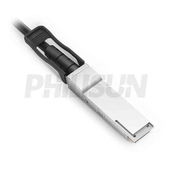
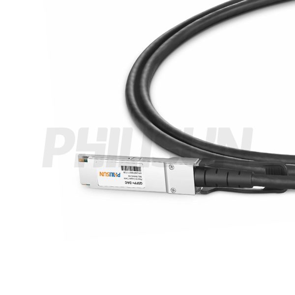
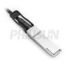
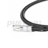
56G QSFP+ to QSFP+ Passive Direct Attach Copper Twinax Cable (DAC)
Compliant with IEEE802.3ba、SFF-8436 MSA standard
Switch to Switch
Switch to GPU
- High Quality
- Factory Outlet
- Satisfaction Guarantee
- Global Shipping
| SPECIFICATIONS | |||
|---|---|---|---|
| Cable End Connector A | QSFP+ | Cable End Connector B | QSFP+ |
| Jumper Type | Direct-Attach | Data Rate | 56G |
| Aggregate Bit Rate | 56Gbps | Lane Bit Rate | 16Gbps |
| Number of Channels | 4 | Single Channel Rate | 16G |
| Minimum Bend Radius | 5X Cable OD -Single, 10X Cable OD - Repeated | Factory Brand | PHILISUN |
| Attenuation | 26AWG:10dB/8.5m maximum 30AWG:8.4dB/5.5m maximum | Bit Error Rate | ≤10-12 |
| Shield | Braid/Foil | Wire AWG | 26AWG/30AWG |
| Cable Type | Passive Twinax | Cable OD | 30AWG: 6.0mm 26AWG: 7.8mm |
| Cable Colour/Material | Black PVC(OFNR) | Cable Length Selection | 0.5-5 meter |
| Protocols | SFF-8436/40G InfiniBand 4x FDR/IEEE802.3ba | Application Scenarios | 56Gigabit Ethernet (56GbE) |
| Supply Voltage | 3.3V | Power Dissipation | <0.5W |
| Operating Temperature | 0 to 70℃ (32 to 158℉) | Storage Temperature | -40 to 85℃ (-40 to 185℉) |
PRODUCT PRESENTATION
The PHILISUN 56G QSFP+ to QSFP+ Passive Direct Attach Copper Twinax Cable (DAC) provides a reliable, high-speed, point-to-point link, optimized for InfiniBand (FDR) and 56GbE protocols in Data Center and HPC environments. Engineered for the lowest power consumption and Ultra-Low Latency, this Passive Copper solution is fully compliant with the IEEE802.3ba and SFF-8436 MSA Standard. It is a Cost-Effective copper twinax alternative, supporting critical links from Switch to Switch and accelerating data transfer for Switch to GPU interconnects over short distances.
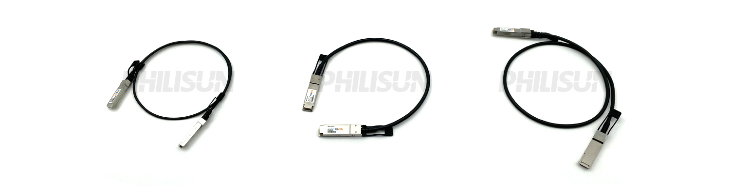
DAC SERIES PRODUCTS
PRODUCTION & TESTING EQUIPMENT

PERFORMANCE PARAMETER
| Absolute Maximum Ratings | |||||||||
| Parameter | Symbol | Min | Typ. | Max | Unit | Ref. | |||
| Storage Temperature | Ts | -40 | – | 85 | ℃ | – | |||
| Supply Voltage | VCCT, R | -0.5 | – | 4 | V | – | |||
| Relative Humidity | Vcc | 0 | – | 85 | % | – | |||
| Recommended Operating Environment | |||||||||
| Parameter | Symbol | Min | Typ. | Max | Unit | Ref. | |||
| Caseoperating Temperature | Tc | 0 | – | 70 | ℃ | – | |||
| Supply Voltage | VCCT, R | 3.13 | 3.3 | 3.47 | V | – | |||
| Power Dissipation | PD | – | – | 0.02 | W | – | |||
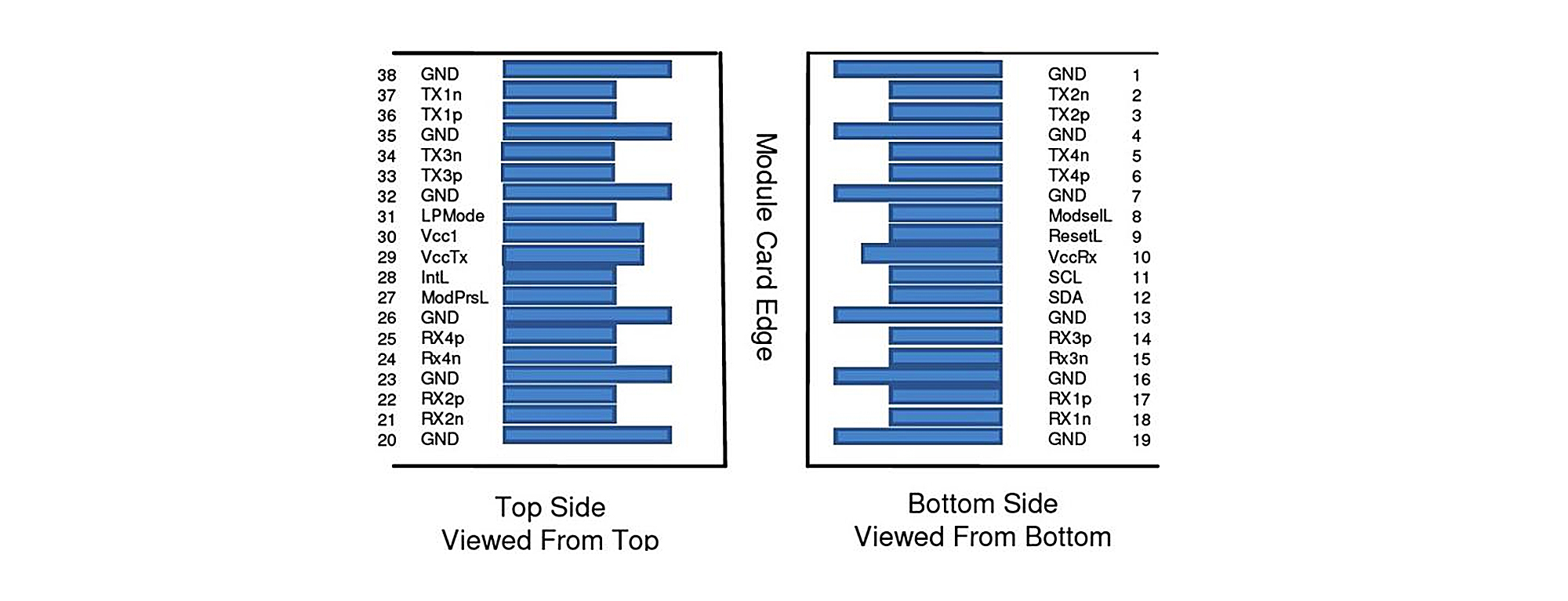
Pin Assignment
| PIN | Logic | Symbol | Description | Notes | |||||
| 1 | – | GND | Ground | 1 | |||||
| 2 | CML-I | Tx2n | Transmitter Inverted Data Input | – | |||||
| 3 | CML-I | Tx2p | Transmitter Non-Inverted Data Input | – | |||||
| 4 | – | GND | Ground | 1 | |||||
| 5 | CML-I | Tx4n | Transmitter Inverted Data Input | – | |||||
| 6 | CML-I | Tx4p | Transmitter Non-Inverted Data Input | – | |||||
| 7 | – | GND | Ground | 1 | |||||
| 8 | LVTTL-I | ModSelL | Module Select | – | |||||
| 9 | LVTTL-I | ResetL | Module Reset | – | |||||
| 10 | – | VccRx | +3.3 V Power Supply Receiver | 2 | |||||
| 11 | LVCMOS-I/O | SCL | 2-wire serial interface clock | – | |||||
| 12 | LVCMOS-I/O | SDA | 2-wire serial interface data | – | |||||
| 13 | – | GND | Ground | 1 | |||||
| 14 | CML-O | Rx3p | Receiver Non-Inverted Data Output | – | |||||
| 15 | CML-O | Rx3n | Receiver Inverted Data Output | – | |||||
| 16 | – | GND | Ground | 1 | |||||
| 17 | CML-O | Rx1p | Receiver Non-Inverted Data Output | – | |||||
| 18 | CML-O | Rx1n | Receiver Inverted Data Output | – | |||||
| 19 | – | GND | Ground | 1 | |||||
| 20 | – | GND | Ground | 1 | |||||
| 21 | CML-O | Rx2n | Receiver Inverted Data Output | – | |||||
| 22 | CML-O | Rx2p | Receiver Non-Inverted Data Output | – | |||||
| 23 | – | GND | Ground | 1 | |||||
| 24 | CML-O | Rx4n | Receiver Inverted Data Output | – | |||||
| 25 | CML-O | Rx4p | Receiver Non-Inverted Data Output | – | |||||
| 26 | – | GND | Ground | 1 | |||||
| 27 | LVTTL-O | ModPrsL | Module Present | – | |||||
| 28 | LVTTL-O | IntL | Interrupt | – | |||||
| 29 | – | VccTx | +3.3V Power supply transmitter | 2 | |||||
| 30 | – | Vcc1 | +3.3V Power supply | 2 | |||||
| 31 | LVTTL-I | LPMode | Low Power Mode | – | |||||
| 32 | – | GND | Ground | 1 | |||||
| 33 | CML-I | Tx3p | Transmitter Non-Inverted Data Input | – | |||||
| 34 | CML-I | Tx3n | Transmitter Non-Inverted Data Output | – | |||||
| 35 | – | GND | Ground | 1 | |||||
| 36 | CML-I | Tx1p | Transmitter Inverted Data Output | – | |||||
| 37 | CML-I | Tx1n | Transmitter Non-Inverted Data Output | – | |||||
| 38 | – | GND | Ground | 1 | |||||
| Notes: 1. GND is the symbol for signal and supply (power) common for the QSFP+ module. All are common within the QSFP+ module and all module voltages are referenced to this potential unless otherwise noted. Connect these directly to the host board signal-common ground plane. 2.Vcc Rx, Vcc1 and VccTx are the receiver and transmitter power supplies and shall be applied concurrently. Vcc Rx Vcc1 and VccTx may be internally connected with- in the QSFP+ Module module in any combination. The connector pins are each rated for a maximum current of 500 mA. |
|||||||||
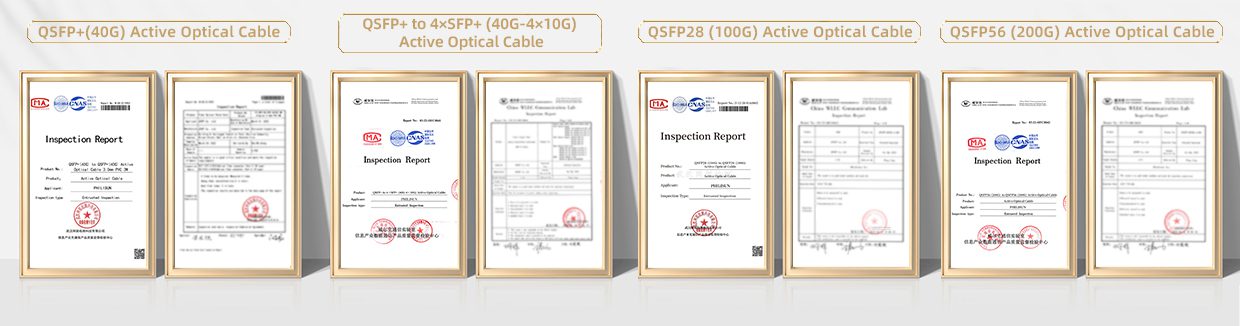
PRODUCT CERTIFICATION
COMPATIBLE BRANDS

CONFIGURATION INFORMATION