

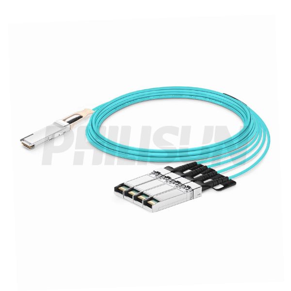
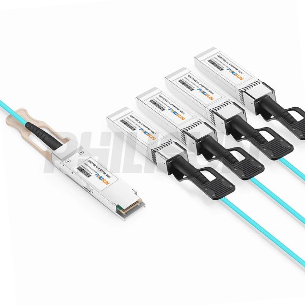


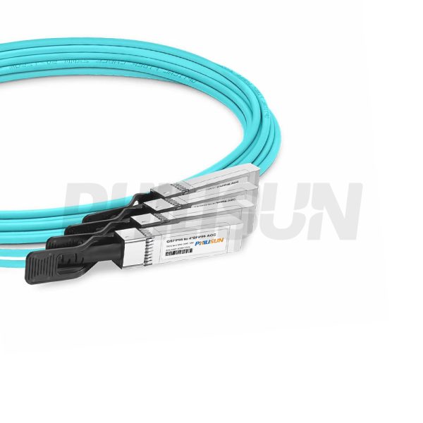
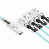
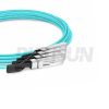
200G QSFP56 to 4×50G SFP56 Active Optical Cable(AOC)
Compliant with the SFF-8436 QSFP56 MSA standard
Switch to Switch
Switch to GPU
- High Quality
- Factory Outlet
- Satisfaction Guarantee
- Global Shipping
| SPECIFICATIONS | |||
|---|---|---|---|
| Cable End Connector A | QSFP56 | Cable End Connector B | 4×SFP56 |
| Jumper Type | Active Optical Breakout Cable | Data Rate | 200G |
| Aggregate Bit Rate | 212.5Gbps | Lane Bit Rate | 53.125Gbps |
| Number of Channels | 4 | Single Channel Rate | 50G |
| Array Transmitter | VSCEL | Array Receiver | PIN |
| Minimum Bend Radius | 30mm | Factory Brand | PHILISUN |
| Center(Operating) Wavelength | 850nm | Bit Error Rate | 2.4E-4 |
| Fiber Type | OM3 MMF MAX 70m | Cable Colour | Aqua |
| Cable Material | LSZH/OFNP | Cable Length Selection | 1-70meter |
| Safety Certification | TUV/UL/FDA | Application Scenarios | 200 Gigabit Ethernet (200GbE) |
| Protocols | QSFP56 MSA/SFP56 MSA | DDMI(Commercial) | YES |
| Supply Voltage | 3.3V | Power Dissipation | QSFP56:<5.5W SFP56:<3.0W |
| Operating Temperature | 0 to 70℃ (32 to 158℉) | Storage Temperature | -20 to 85℃ (-4 to 185℉) |
PRODUCT PRESENTATION
The PHILISUN 200G QSFP56 to 4×50G SFP56 Active Optical Breakout Cable is a direct-attach fiber assembly designed for linking 200G devices to 50G devices. The product complies with SFF-8436, SFF-8431, and MSA standards and is suitable for heterogeneous connections across adjacent racks. It uses OM3 Multimode Fiber. Its compact structure and fully sealed integrated optics reduce costs compared to conventional optical modules and jumpers, while significantly improving reliability and reducing maintenance. This AOC guarantees broad compatibility with major vendor platforms including Cisco, H3C, Huawei, Juniper, and Arista, and more.
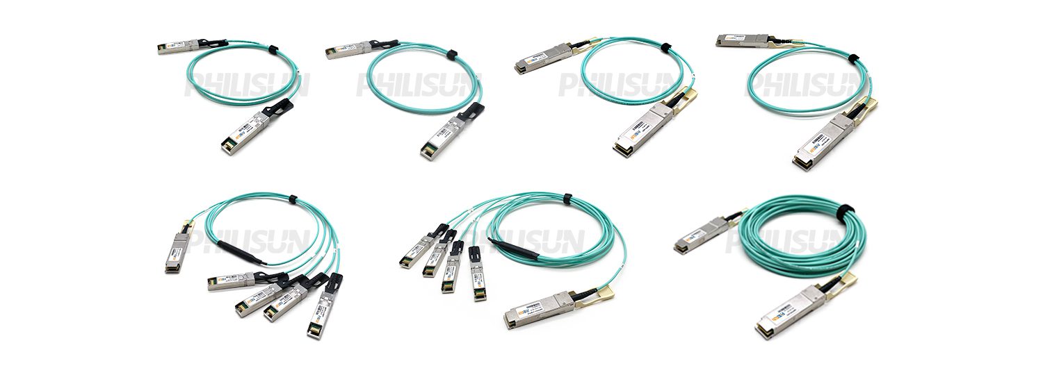
AOC SERIES PRODUCTS
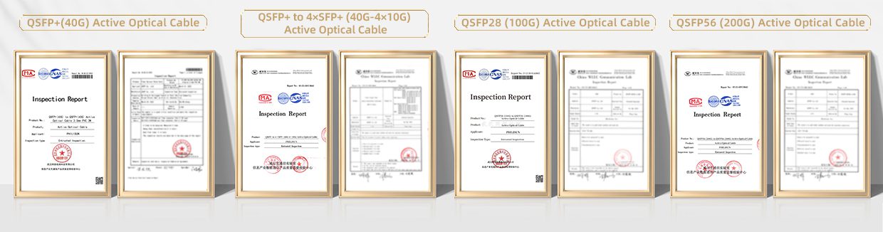
PRODUCTION & TESTING EQUIPMENT

PERFORMANCE PARAMETER
| Absolute Ratings | |||||||||
| Parameter | Symbol | Min | Max | Unit | |||||
| Storage Temperature | Tc | -40 | + 85 | ℃ | |||||
| Case Operating Temperature | Tc | 0 | +70 | ℃ | |||||
| Supply Voltage | VccT, R | – | 3.3 | V | |||||
| Relative Humidity | RH | 0 | 85 | % | |||||
| Recommended Operating Environment | |||||||||
| Parameter | Min | Max | Unit | ||||||
| Supply Voltage | 3.15 | 3.3 | V | ||||||
| Supply current QSFP56 end | – | 1660 | mA | ||||||
| Supply current SFP56 end | – | 900 | mA | ||||||
| Data Rate Per Lane | – | 53.125 | Gbps | ||||||
| Fiber Bend Radius | 30 | – | mm | ||||||
| Transmitter Specifications | |||||||||
| Parameter | Min | Max | Unit | ||||||
| Input differential impedance | 90 | 110 | Ω | ||||||
| Differential Input Voltage swing, per lane | 300 | 1100 | mV | ||||||
| Transmit Disable Voltage | 2.0 | VCC+0.3 | V | ||||||
| Transmit Enable Voltage | Vee | Vee+0.8 | V | ||||||
| Receiver Specifications | |||||||||
| Parameter | Min | Max | Unit | ||||||
| Differential Output Swing, per lane | 300 | 900 | mV | ||||||
| Bit Error Rate@53.125 Gbps | – | 2.4E-4 | – | ||||||
| Bit Error Rate@25.78125 Gbps | – | 5E-5 | – | ||||||
| Output Differential Impedance | 90 | 110 | Ω | ||||||
| Loss of Signal -Asserted | 2.0 | VCC+0.3 | V | ||||||
| Loss of Signal -Negated | Vee | Vee+0.8 | V | ||||||
TRANSCEIVER ELECTRICAL PAD LAYOUT(QSFP56 end)
PIN DESCRIPTION(QSFP56 end)
| Pin | Name | Name/Description | |||||||
| 1 | GND | Ground | |||||||
| 2 | Tx2n | Transmitter Inverted Data Input | |||||||
| 3 | Tx2p | Transmitter Non-Inverted Data Input | |||||||
| 4 | GND | Ground | |||||||
| 5 | Tx4n | Transmitter Inverted Data Input | |||||||
| 6 | Tx4p | Transmitter Non-Inverted Data Input | |||||||
| 7 | GND | Ground | |||||||
| 8 | ModSelL | Module Select | |||||||
| 9 | ResetL | Module Reset | |||||||
| 10 | Vcc Rx | +3.3 V Power supply receiver | |||||||
| 11 | SCL | 2-wire serial interface clock | |||||||
| 12 | SDA | 2-wire serial interface data | |||||||
| 13 | GND | Ground | |||||||
| 14 | Rx3p | Receiver Non-Inverted Data Output | |||||||
| 15 | Rx3n | Receiver Inverted Data Output | |||||||
| 16 | GND | Ground | |||||||
| 17 | Rx1p | Receiver Non-Inverted Data Output | |||||||
| 18 | Rx1n | Receiver Inverted Data Output | |||||||
| 19 | GND | Ground | |||||||
| 20 | GND | Ground | |||||||
| 21 | Rx2p | Receiver Inverted Data Output | |||||||
| 22 | GND | Receiver Non-Inverted Data Output | |||||||
| 23 | Rx4n | Ground | |||||||
| Pin | Name | Name/Description | |||||||
| 24 | Rx4n | Receiver Inverted Data Output | |||||||
| 25 | Rx4p | Receiver Non-Inverted Data Output | |||||||
| 26 | GND | Ground | |||||||
| 27 | Mod PrsL | Module Present | |||||||
| 28 | IntL | Interrupt | |||||||
| 29 | VCC Tx | +3.3 V Power supply transmitter | |||||||
| 30 | VCC1 | +3.3 V Power Supply | |||||||
| 31 | LPMode | Low Power Mode | |||||||
| 32 | GND | Ground | |||||||
| 33 | Tx3p | Transmitter Non-Inverted Data Input | |||||||
| 34 | Tx3n | Transmitter Inverted Data Input | |||||||
| 35 | GND | Ground | |||||||
| 36 | Tx1p | Transmitter Non-Inverted Data Input | |||||||
| 37 | Tx1n | Transmitter Inverted Data Input | |||||||
| 38 | GND | Ground | |||||||
TRANSCEIVER ELECTRICAL PAD LAYOUT(SFP56 end)
![]()
PIN DESCRIPTION(SFP56 end)
| Pin | Name | Name/Description | |||||||
| 1 | VEET | Transmitter Ground | |||||||
| 2 | Tx_FAULT | Transmitter Fault | |||||||
| 3 | Tx_DIS | Transmitter Disable. Laser output disabled on high or open | |||||||
| 4 | SDA | 2-wire Serial Interface Data Line | |||||||
| 5 | SCL | 2-wire Serial Interface Clock Line | |||||||
| 6 | MOD_ABS | Module Absent. Grounded within the module | |||||||
| 7 | RS0 | Rate Select 0 | |||||||
| Pin | Name | Name/Description | |||||||
| 8 | RX_LOS | Loss of Signal indication. Logic 0 indicates normal operation | |||||||
| 9 | RS1 | Rate Select 1 | |||||||
| 10 | VEER | Receiver Ground | |||||||
| 11 | VEER | Receiver Ground | |||||||
| 12 | RD- | Receiver Inverted DATA out. AC Coupled | |||||||
| 13 | RD+ | Receiver DATA out. AC Coupled | |||||||
| 14 | VEER | Receiver Ground | |||||||
| 15 | VCCR | Receiver Power Supply | |||||||
| 16 | VCCT | Transmitter Power Supply | |||||||
| 17 | VEET | Transmitter Ground | |||||||
| 18 | TD+ | Transmitter DATA in. AC Coupled | |||||||
| 19 | TD- | Transmitter Inverted DATA in. AC Coupled | |||||||
| 20 | VEET | Transmitter Ground | |||||||
PRODUCT CERTIFICATION
COMPATIBLE BRANDS

CONFIGURATION INFORMATION
Related products
-
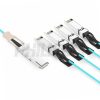
-500x500.jpg "1QSFP56 to 2×QSFP56 (200G-100G)")
200G QSFP56 to 2×100G QSFP56 Active Optical Cable(AOC)
Compliant with the SFF-8665 QSFP56 MSA standard
Switch to Switch
Switch to GPU -

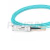
200G QSFP56 to QSFP56 Active Optical Cable (AOC)
Compliant with theSFF-8436 QSFP56 MSA standard
Switch to Switch
Switch to GPU