

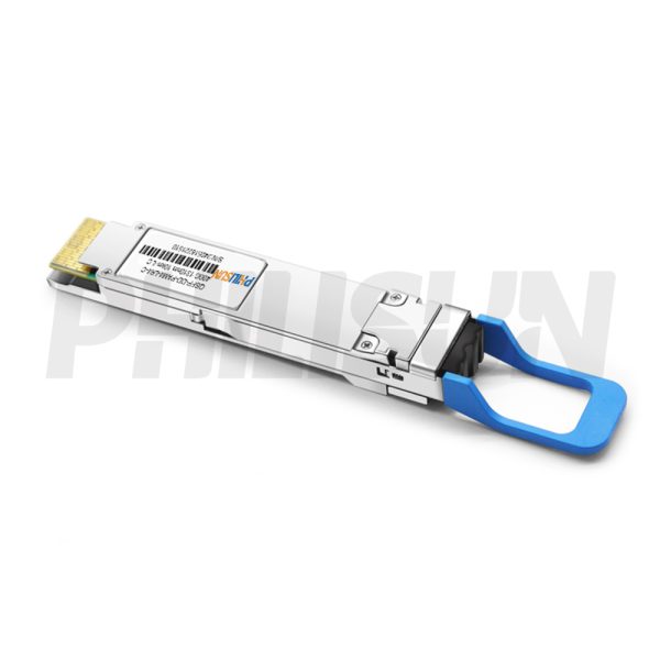
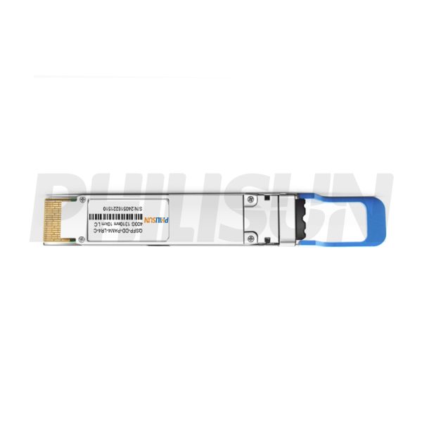
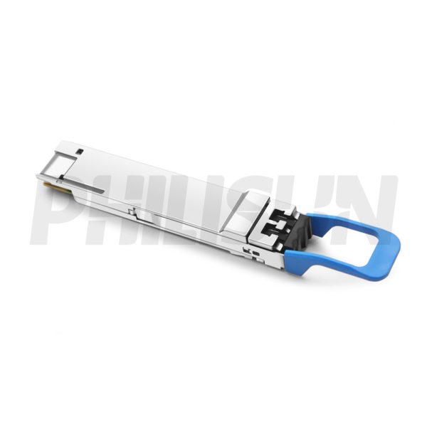
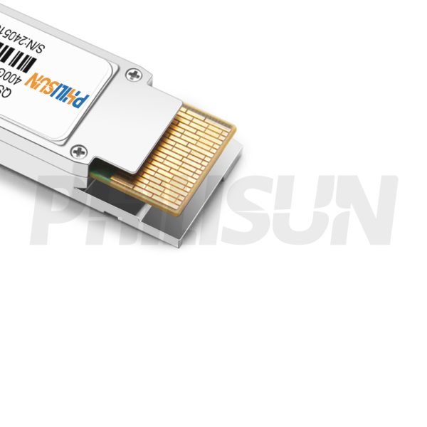
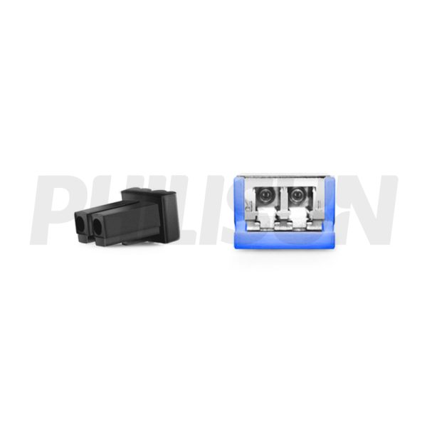
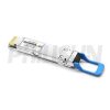
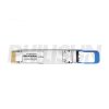

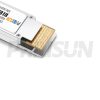
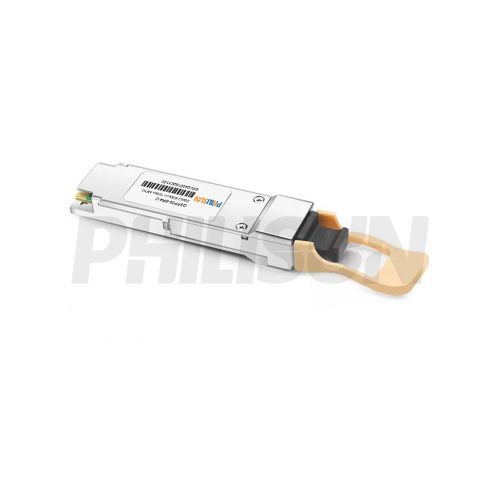
400G QSFP-DD 1310nm 10km DOM Duplex LC SMF Optical Transceiver Module
QSFPDD-400(4×100)-13-10(LR4)-LCD
- High Quality
- Factory Outlet
- Satisfaction Guarantee
- Global Shipping
| SPECIFICATIONS | |||
|---|---|---|---|
| Product Model | QSFPDD-400(4x100)-13-10(LR4)-LCD | Manufacturer brand | PHILISUN |
| Package Type | QSFPDD | Optical connector | LC DX |
| Max Data Rate | 400Gbps | Channel Data Rate | 53.125Gbps |
| Effective transmission distance | 10km | ||
| Wavelength | 1310nm | Operating voltage | 3.3V |
| Fiber Type | SMF | Core Size | 9/125 |
| Transmitter Type | CWDM EML | Receiver Type | PIN |
| TX Power | -2.8~4dBm | Receiver Sensitivity | -6.8dBm |
| Digital Optical Monitoring(DOM) | YES | Receiver Overload | 4dBm |
| Power Consumption | <10W | Protocols | 400G Ethernet Infiniband interconnect Data center Enterprise Networking |
| Operating temperature(Commercial) | 0℃~+70℃ | Storage Temperature(Commercial) | -40℃~+85℃ |
PRODUCT PRESENTATION
The PHILISUN QSFP-DD 400G (4x100G) 1310nm 10km LR4 LC DX Transceiver is a high-performance 400Gb/s Quad Small Form Factor Pluggable-Double Density (QSFP-DD) optical module designed for optical communication over distances up to 10km. This module converts 8 channels of 50Gb/s (PAM4) electrical input into 4 CWDM optical signals, multiplexing them into a single channel for 400Gb/s optical transmission. On the receiver side, it de-multiplexes the 400Gb/s optical input into 4 CWDM optical signals and converts them back into 8 channels of 50Gb/s (PAM4) electrical output.The 4 CWDM channels have central wavelengths of 1271nm, 1291nm, 1311nm, and 1331nm, as defined by the CWDM wavelength grid in ITU-T G.694.2. The transceiver features a duplex LC connector for the optical interface and a 76-pin connector for the electrical interface. To ensure optimal performance over long distances, single-mode fiber (SMF) must be used.Additionally, host Forward Error Correction (FEC) is required to support transmission distances of up to 10km.This module is designed for reliability and efficiency, making it an ideal solution for high-speed, long-range optical communication in advanced network systems.
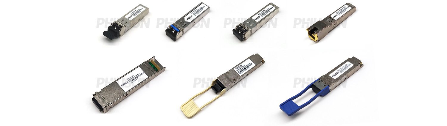
TRANSCEIVER SERIES PRODUCTS
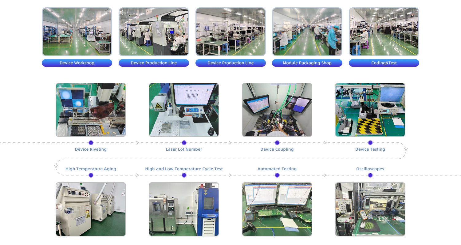
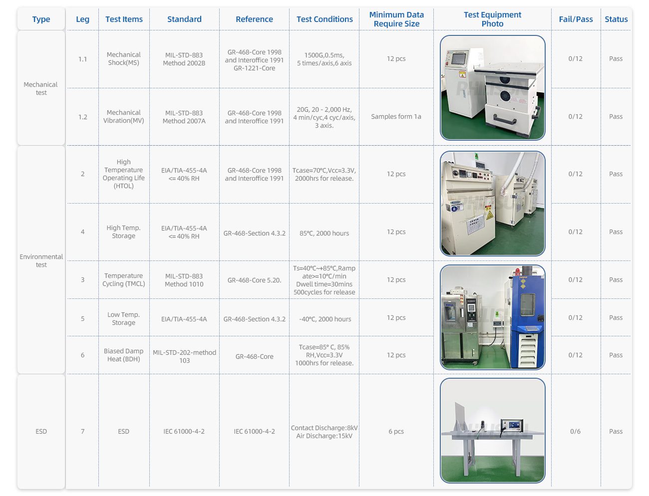
PRODUCTION & TESTING EQUIPMENT
PERFORMANCE PARAMETER
| Absolute Maximum Ratings | |||||||||
| Parameter | Symbol | Min. | Max. | Unit | |||||
| Power supply voltage | VCC | -0.5 | +3.6 | V | |||||
| Storage temperature | TC | -40 | +85 | °C | |||||
| Relative humidity | RH | 0 | 85 | % | |||||
| These values represent the damage threshold of the module.Stress in excess of any of theindividual absolute maximum ratings can cause immediate catastrophic damage to the module even if all other parameters are within recommended operating conditions. | |||||||||
| Recommended Operating Environment | |||||||||
| Parameter | Symbol | Min. | Typical | Max | Unit | ||||
| Power supply voltage | VCC | 3.135 | 3.30 | 3.465 | V | ||||
| Operating case temperature | Tca | 0 | – | 70 | ℃ | ||||
| Recommended operating environment specifies parameters for which the electrical and optical characteristics hold unless otherwise noted. | |||||||||
| Electrical Characteristics | |||||||||
| Parameter | Symbol | Min | Typical | Max | Unit | Notes | |||
| Data rate per lane | DR | 53.125±100ppm | Gbps | – | |||||
| Transmitter | |||||||||
| Input differential impedance | Rin | 90 | 100 | 110 | Ω | – | |||
| Differential input voltage swing | Vin | 900 | – | 1100 | mVp-p | – | |||
| Receiver | |||||||||
| Differential output swing | Vout | – | – | 900 | mVp-p | – | |||
| Output differential impedance | Rout | 900 | 100 | 110 | Ω | – | |||
| The following electrical characteristics are defined over the recommended operating environment unless otherwise specified. | |||||||||
| Optical Characteristics | |||||||||
| Parameter | Symbol | Min | Typical | Max | Unit | Notes | |||
| Transmitter | |||||||||
| Center wavelength | Ch0 | λ0 | 1264.5 | 1271 | 1277.5 | nm | – | ||
| Ch1 | λ1 | 1284.5 | 1291 | 1297.5 | |||||
| Ch2 | λ2 | 1304.5 | 1311 | 1317.5 | |||||
| Ch3 | λ3 | 1324.5 | 1331 | 1337.5 | |||||
| Data rate,each lane | – | 53.125±100ppm | GBd | – | |||||
| Side-mode suppression ratio | SMSR | 30 | – | – | dB | – | |||
| Average optical power,per lane | Po | -2.8 | – | 4.0 | dBm | 1 | |||
| Extinction ratio | ER | 3.5 | – | – | dBm | – | |||
| Transmitter and dispersion eye closure | TDECQ | – | – | 3.9 | dB | – | |||
| Optical return loss tolerance | ORL | – | – | 15.6 | dB | – | |||
| Receiver | |||||||||
| Center wavelength | Ch0 | λ0 | 1264.5 | 1271 | 1277.5 | nm | – | ||
| Ch1 | λ1 | 1284.5 | 1291 | 1297.5 | |||||
| Ch2 | λ2 | 1304.5 | 1311 | 1317.5 | |||||
| Ch3 | λ3 | 1324.5 | 1331 | 1337.5 | |||||
| Data rate,each lane | – | 53.125±100ppm | GBd | – | |||||
| Average receive power,each lane | – | -9.1 | – | 4.0 | dBm | – | |||
| Receive power(OMAouter), each lane |
– | – |
 –
|
4.2 | dBm | – | |||
| Receiver sensitivity(OMAouter), each lane |
– | – | – | -6.8 | dBm | 2 | |||
| LOS asserted | Lsa | -20 | – |
 –
|
dBm | – | |||
| LOS de-asserted | Lda | – | -12.1 | dBm | – | ||||
| LOS hysteresis | Lh | 0.5 | – | – | dB | – | |||
| Note: [1]Average launch power,each lane(min)is informative and not the principal indicator ofsignal strength.A transmitter with launch power below this value cannot be compliant;however,avalue above this does not ensure compliance. [2]Measured with conformance test signal at TP3 for BER=2.4E-4 Pre-FEC |
|||||||||
| The following optical characteristics are defined over the Recommended Operating Environment unless otherwise specified. | |||||||||
QSFP-DD TRANSCEIVER ELECTRICAL PAD LAYOUT
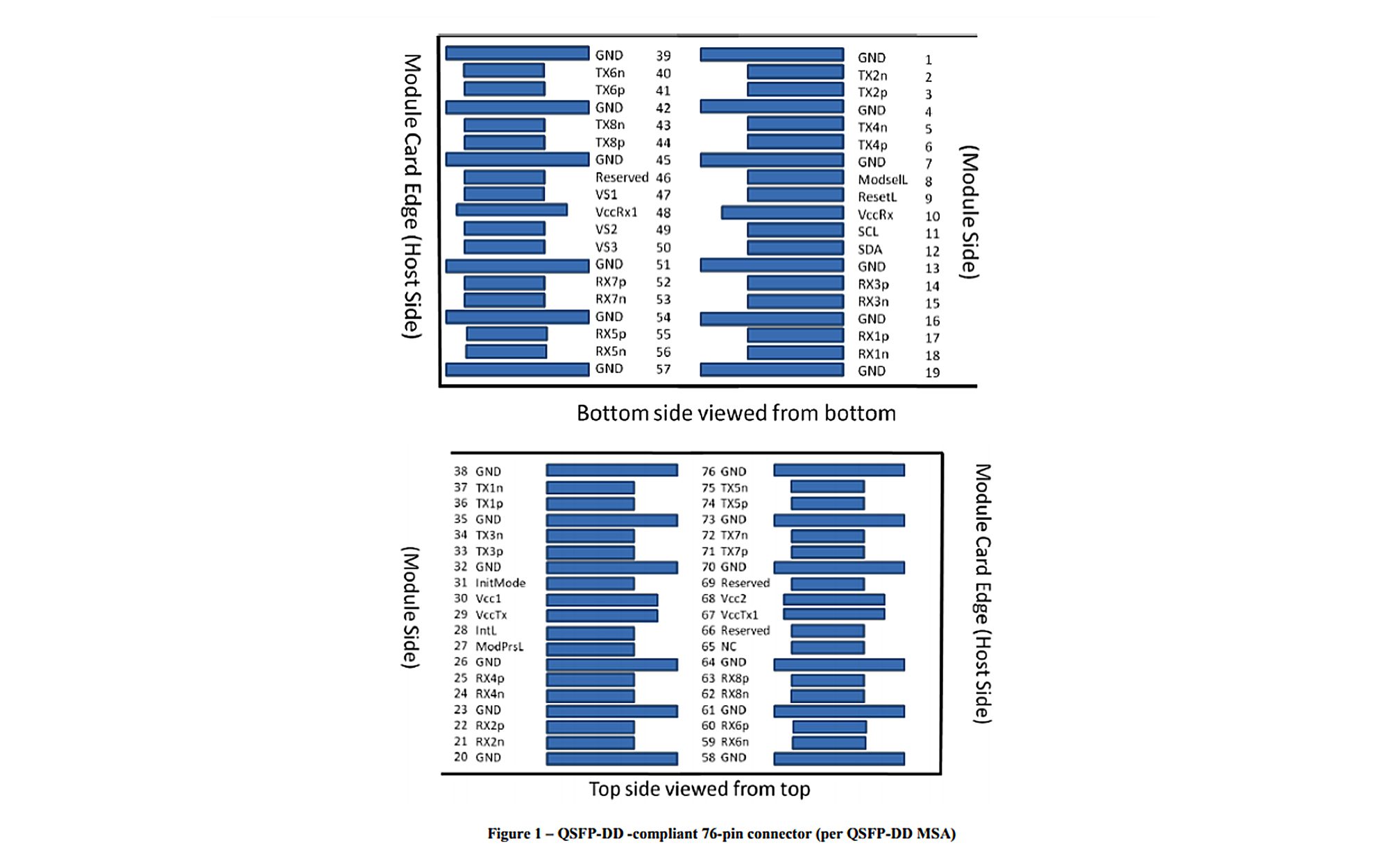
PIN DEFINITION
| Pin Definition | |||||||||
| Pad | Logic | Symbol | Name/Description | ||||||
| 1 | – | GND | Ground | ||||||
| 2 | CML-I | Tx2n | Transmitter inverted data input | ||||||
| 3 | CML-I | Tx2p | Transmitter non-inverted data input | ||||||
| 4 | – | GND | Ground | ||||||
| 5 | CML-I | Tx4n | Transmitter inverted data input | ||||||
| 6 | CML-I | Tx4p | Transmitter non-inverted data input | ||||||
| 7 | – | GND | Ground | ||||||
| 8 | LVTTL-I | ModSelL | Module select | ||||||
| 9 | LVTTL-I | ResetL | Module reset | ||||||
| 10 | – | Vcc Rx | +3.3V Power supply receiver | ||||||
| 11 | LVCMOS- I/0 | SCL | 2-wire serial interface clock | ||||||
| 12 | LVCMOS- I/0 | SDA | 2-wireserial interface data | ||||||
| 13 | – | GND | Ground | ||||||
| 14 | CML-0 | Rx3p | Receiver non-inverted data output | ||||||
| 15 | CML-0 | Rx3n | Receiver inverted data output | ||||||
| 16 | – | GND | Ground | ||||||
| 17 | CML-0 | Rx1p | Receiver non-inverted data output | ||||||
| 18 | CML-0 | Rx1n | Receiver inverted data output | ||||||
| 19 | – | GND | Ground | ||||||
| 20 | – | GND | Ground | ||||||
| 21 | CML-0 | Rx2n | Receiver onverted data output | ||||||
| 22 | CML-0 | Rx2p | Receiver non-inverted data output | ||||||
| 23 | – | GND | Ground | ||||||
| 24 | CML-0 | Rx4n | Receiver inverted data output | ||||||
| 25 | CML-0 | Rx4p | Receiver non-onverted data output | ||||||
| 26 | – | GND | Ground | ||||||
| 27 | LVTTL-0 | ModPrsL | Module present | ||||||
| 28 | LVTTL-0 | IntL | Interrupt | ||||||
| 29 | – | VCC Tx | +3.3V power supply transmitter | ||||||
| 30 | – | VCC1 | +3.3V power supply | ||||||
| 31 | LVTTL-I | InitMode | Initialization mode;in legacy QSFP applications,the initMode pad is called LPMODE | ||||||
| 32 | – | GND | Ground | ||||||
| 33 | CML-I | Tx3p | Transmitter non-inverted data input | ||||||
| 34 | CML-I | Tx3n | Transmitter inverted data input | ||||||
| 35 | – | GND | Ground | ||||||
| 36 | CML-I | Tx1p | Transmitter non-Inverted data input | ||||||
| 37 | CML-I | Tx1n | Transmitter inverted data input | ||||||
| 38 | – | GND | Ground | ||||||
| 39 | – | GND | Ground | ||||||
| 40 | CML-I | Tx6n | Transmitter inverted data input | ||||||
| 41 | CML-I | Tx6p | Transmitter non-inverted data input | ||||||
| 42 | – | GND | Ground | ||||||
| 43 | CML-I | Tx8n | Transmitter inverted data input | ||||||
| 44 | CML-I | Tx8p | Transmitter non-inverted data input | ||||||
| 45 | – | GND | Ground | ||||||
| 46 | – | Reserved | For future use | ||||||
| 47 | – | VS1 | Module vender specific1 | ||||||
| 48 | – | Vcc Rx1 | 3.3V power supply receiver | ||||||
| 49 | – | VS2 | Module vender specific2 | ||||||
| 50 | – | VS3 | Module vender specific3 | ||||||
| 51 | – | GND | Ground | ||||||
| 52 | CML-0 | Rx7p | Receiver non-inverted data output | ||||||
| 53 | CML-0 | Rx7n | Receiver inverted data output | ||||||
| 54 | – | GND | Ground | ||||||
| 55 | CML-0 | Rx5p | Receiver non-inverted data output | ||||||
| 56 | CML-0 | Rx5n | Receiver inverted data output | ||||||
| 57 | – | GND | Ground | ||||||
| 58 | – | GND | Ground | ||||||
| 59 | CML-0 | Rx6n | Receiver inverted data output | ||||||
| 60 | CML-0 | Rx6p | ReceiverNon-inverted data output | ||||||
| 61 | – | GND | Ground | ||||||
| 62 | CML-0 | Rx8n | Receiver inverted data output | ||||||
| 63 | CML-0 | Rx8p | Receiver non-inverted data output | ||||||
| 64 | – | GND | Ground | ||||||
| 65 | – | NC | No connect | ||||||
| 66 | – | Reserved | For futureuse | ||||||
| 67 | – | VCC Tx1 | 3.3V power supply transmitter | ||||||
| 68 | – | VCC2 | 3.3V power supply | ||||||
| 69 | – | Reserved | For future use | ||||||
| 70 | – | GND | Ground | ||||||
| 71 | CML-I | Tx7p | Transmitter non-inverted data input | ||||||
| 72 | CML-I | Tx7n | Transmitter inverted data input | ||||||
| 73 | – | GND | Ground | ||||||
| 74 | CML-I | Tx5p | Transmitter non-inverted data input | ||||||
| 75 | CML-I | Tx5n | Transmitter inverted data input | ||||||
| 76 | – | GND | Ground | ||||||
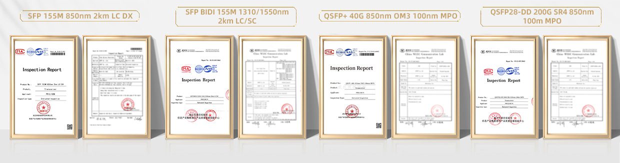
PRODUCT CERTIFICATION
QUALITY ADVANTAGE
COMPATIBLE BRANDS

CONFIGURATION INFORMATION
Related products
-
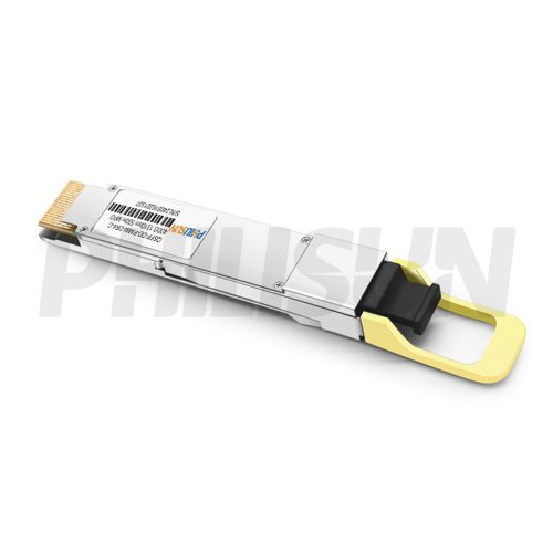
400G QSFP-DD 1310nm 500m DOM MPO8/12 SMF Optical Transceiver Module
QSFPDD-400(4×100)-13-05(DR4)-MPO8/12
-
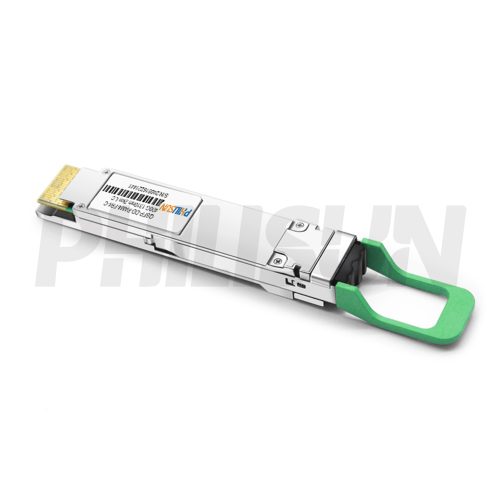
400G QSFP-DD 1310nm 2km DOM Duplex LC SMF Optical Transceiver Module
QSFPDD-400(4×100)-13-2(FR4)-LCD
-
400GBASE-SR8 QSFP-DD 850nm 100m DOM MPO16 MMF Transceiver
QSFPDD-400-85-01(SR8)-MPO16