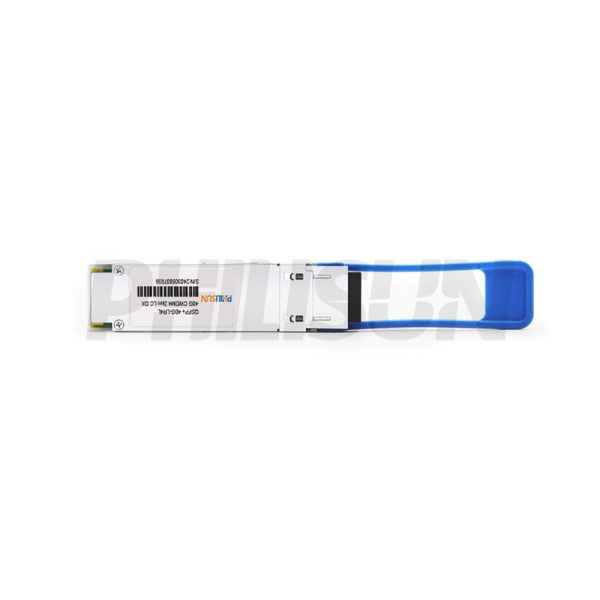
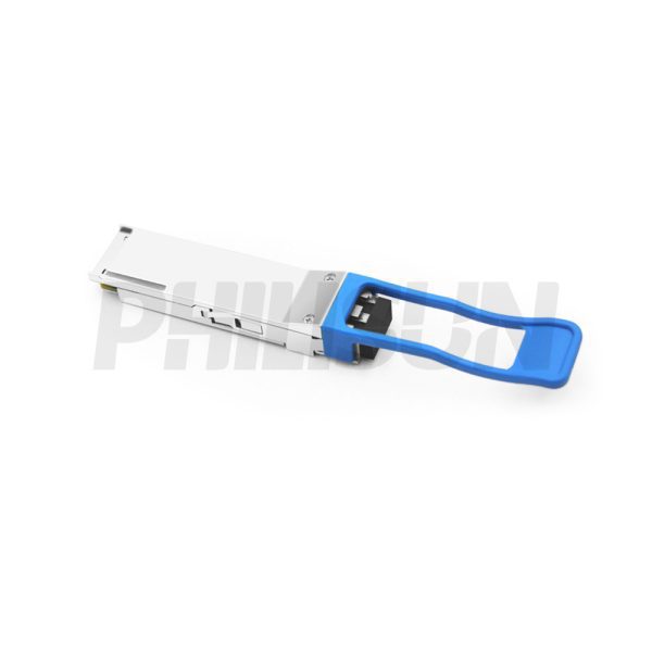
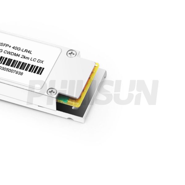
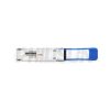
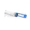
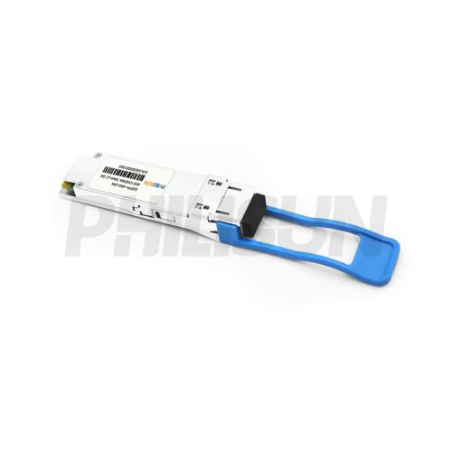
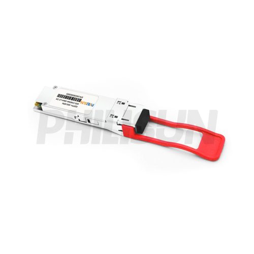
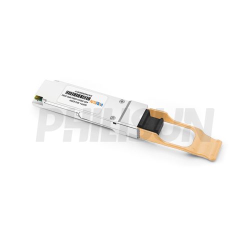
Generic Compatible 40GBASE-LR4L QSFP+ 2km DOM Duplex LC SMF Optical Transceiver Module
QSFP+40-CW4-2(LR4L)-LCD
- High Quality
- Factory Outlet
- Satisfaction Guarantee
- Global Shipping
| SPECIFICATIONS | |||
|---|---|---|---|
| Product Model | QSFP+40-CW4-2(LR4L)-LCD | Manufacturer Brand | PHILISUN |
| Package Type | QSFP+ | Optical Connector | LC Duplex |
| Max Data Rate | 40G | Channel Data Rate | 11.2Gbps |
| Effective Transmission Distance | 2km | ||
| Wavelength | 1271nm 1291nm 1311nm 1331nm | Operating Voltage | 3.3V |
| Fiber Type | SMF | Core Size | 9/125µm |
| Transmitter Type | 4 Lanes CWDM DFB | Receiver Type | PIN |
| TX Power | -7~+2.3dBm | Receiver Sensitivity | < -12dBm |
| Digital Diagnostic Monitoring(DDM) | YES | Receiver Overload | 2.3dBm |
| Power Consumption | ≤3.5W | Protocols | IEEE802.3ba 40GBASE-IR4 Standard |
| Operating temperature(Commercial) | 0℃~+70℃ | Storage Temperature(Commercial) | -40℃~+85℃ |
PRODUCT PRESENTATION
The PHILISUN QSFP+ 40G CWDM4 2km LR4L LC DX transceiver modules are designed for 40 Gigabit per second links over single-mode fiber, compliant with the QSFP+ MSA and IEEE 802.3ba 40GBASE-LR4 standards. They support digital diagnostics via the I2C interface as outlined in the QSFP+ MSA. Additionally, these optical transceivers adhere to the RoHS Directive 2011/65/EU for environmental safety compliance.
TRANSCEIVER SERIES PRODUCTS

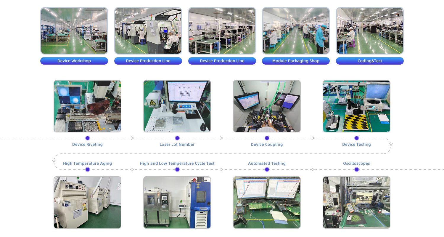
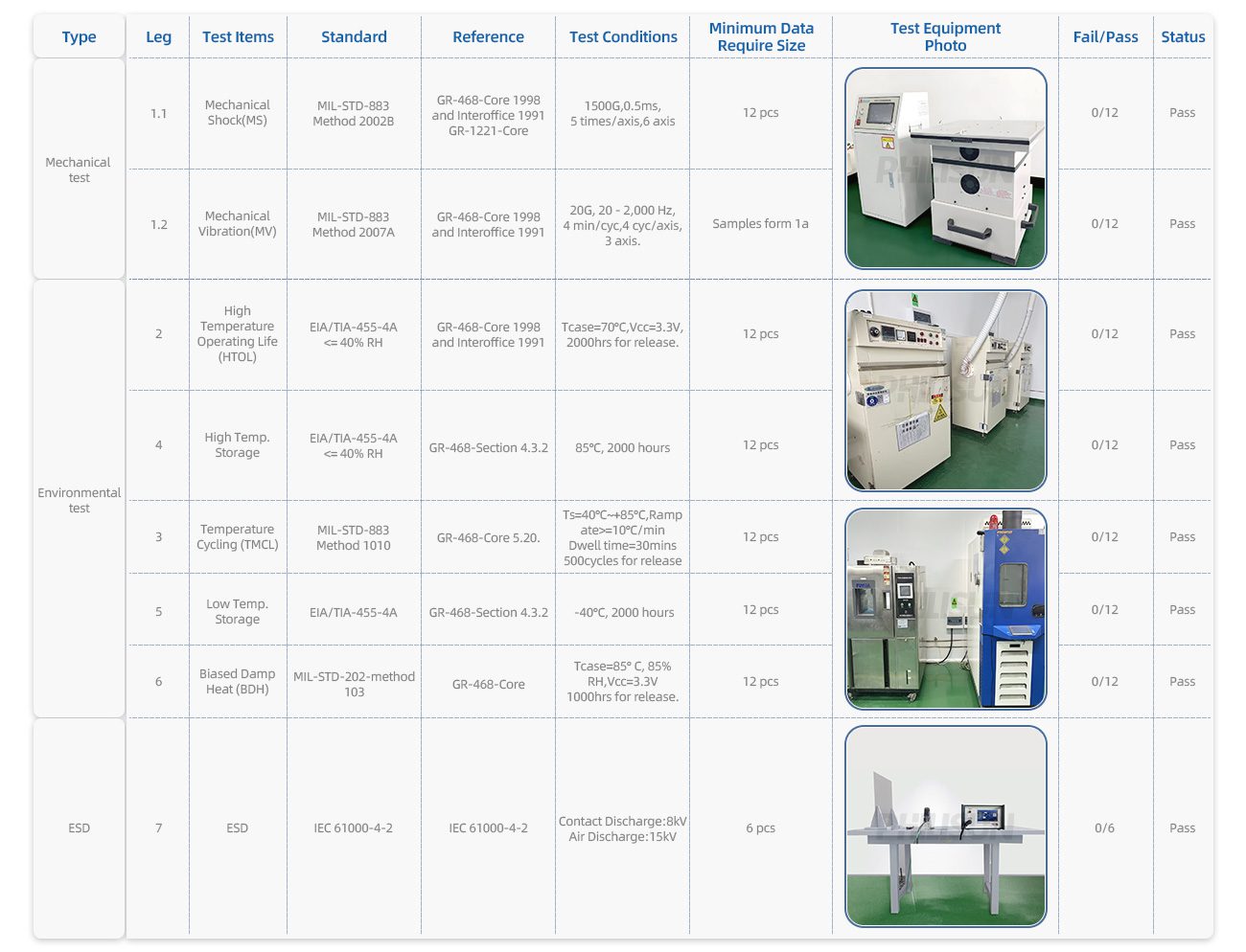
PRODUCTION & TESTING EQUIPMENT
PERFORMANCE PARAMETER
| General Specifications | |||||||||
| Parameter | Value | Unit | Notes | ||||||
| Module Form Factor | QSFP+ | – | – | ||||||
| Number of Lanes | 4 Tx and 4 | – | – | ||||||
| Maximum Aggregate Data Rate | 41.2 | Gb/s | – | ||||||
| Maximum Data Rate per Lane | 10.3 | Gb/s | Higher bit rates may be supported. Please contact FS. | ||||||
| Protocols Supported | Typical applications include 40G Ethernet, Infiniband Fibre Channel, SATA/SAS3 | – | – | ||||||
| Electrical Interface and Pin-out | 38-pin edge connector | – | Pin-out as defined by the QSFP+ MSA | ||||||
| Maximum Power Consumption | 3.5 | – | – | ||||||
| Management Interface | Serial, I2C-based, 400 kHz maximum frequency | As defined by the QSFP+ MSA | |||||||
| Data Rate Specifications | Symbol | Min | Typ. | Max | Units | Ref. | |||
| Bit Rate per Lane | BR | – | – | 10313 | Mb/sec | 1 | |||
| Bit Error Ratio | BER | – | – | 10-12 | – | 2 | |||
| Link distance on SMF-28 | d | – | – | 2 | kilometers | 3 | |||
| Notes: 1.Compliant with 40GBASE-LR4 and XLPPI per IEE 802.3ba. Compatible with 1/10 Gigabit Ethernet and 1/2/4/8/10G Fibre Channel. 2.Tested with a PRBS 231-1 test pattern. 3.Per 40GBASE-LR4, IEEE 802.3ba. |
|||||||||
| Absolute Maximum Ratings | |||||||||
| Parameter | Symbol | Min | Typ. | Max | Unit | Ref. | |||
| Maximum supply voltage | Vcc1, VccTx, VccRx | -0.5 | – | 3.6 | V | – | |||
| Supply voltage | Ts | -40 | – | +85 | °C | – | |||
| Case operating temperature | Top | +15 | – | +60 | °C | – | |||
| Relative humidity | RH | 0 | – | 85 | % | 1 | |||
| Damage threshold, per lane | DT | 3.4 | – | – | dBm | – | |||
| Note: 1.Non-condensing. |
|||||||||
| Electrical Characteristics | |||||||||
| Parameter | Symbol | Min | Typ. | Max | Unit | Ref. | |||
| Supply voltage | Vcc1, VccTx, VccRx | 3.1 | – | 3.47 | V | – | |||
| Supply current | Icc | – | – | 1.13 | A | – | |||
| Transmit turn-on time | – | – | – | 2000 | ms | 1 | |||
| Transmitter (per lane) | |||||||||
| Single ended input voltage tolerance | VinT | -0.3 | – | 4.0 | V | – | |||
| Differential data input swing | Vin,pp | 120 | – | 1200 | mVpp | 2 | |||
| Differential input threshold | – | – | 50 | – | mV | – | |||
| AC common mode input voltage tolerance (RMS) | – | 15 | – | – | mV | – | |||
| J2 jitter tolerancez | Jt2 | 0.17 | – | – | UI | – | |||
| J9 jitter tolerance | Jt9 | 0.29 | – | – | UI | – | |||
| Data dependent pulse width shrinkage | DDPWS | 0.07 | – | – | UI | – | |||
| Eye mask colordinates {X1, X2 ,Y1, Y2} |
– | – | 0.11, 0.31 95, 350 |
– | UI mV |
4 | |||
| Receiver (per lane) | |||||||||
| Single-ended output voltage | – | -0.3 | – | 4.0 | V | – | |||
| Differential data output swing | Vout,pp | 200 | – | 400 | mVpp | 5,6 | |||
| 300 | – | 600 | |||||||
| 400 | 550 | 800 | |||||||
| 600 | – | 1200 | |||||||
| AC common mode output voltage (RMS) | – | – | – | 7.5 | mV | – | |||
| Termination mismatch at 1 MHx | – | – | – | 5 | % | – | |||
| Differential output return loss | – | Per IEEE P802.3ba,Section 86A.4.2.1 | dB | 3 | |||||
| Common mode output return loss | – | Per IEEE P802.3ba,Section 86A.4.2.2 | dB | 3 | |||||
| Output transition time, 20% to 80% | – | 28 | – | – | ps | – | |||
| J2 jitter output | Jo2 | – | – | 0.42 | UI | – | |||
| J9 jitter output | Jo9 | – | – | 0.65 | UI | – | |||
| Eye mask coordinates #1 {X1, X2, Y1, Y2} |
– | – | 0.29, 0.5 150, 425 |
– | UI mV |
4 | |||
| Power supply ripple tolerance | PSR | 50 | – | – | mVpp | – | |||
| Notes: 1.From power-on and end of any fault conditions. 2.After internal AC coupling. Self-biasing 100Ωdifferential input. 3.10 MHz to 11.1 GHz range 4.Hit ratio = 5 x 10E-5. 5.AC coupled with 100Ωdifferential output impedance. 6.Output voltage is settable in 4 discrete steps via the I2C. Default is 400-800 mV. |
|||||||||
| Optical Characteristics | |||||||||
| Parameter | Symbol | Min | Typ. | Max | Unit | Ref. | |||
| Transmitter (per lane) | |||||||||
| Signaling speed per lane | – | – | – | 10.3125 | GBd | 1 | |||
| Lane center wavelengths (range) | – | 1264.5-1277.5 1284.5-1297.5 1304.5-1317.5 1324.5-1337.5 |
nm | – | |||||
| Total average launch power | Pout | – | – | 8.3 | dBm | – | |||
| Average launch power per lane | TXPx | -7.0 | – | 2.3 | dBm | – | |||
| Transmit OMA per lane | TxOMA | -4.0 | – | 3.5 | dBm | 2 | |||
| Optical extinction ratio |
ER
|
3.5 | – | – | dB | – | |||
| Sidemode suppression ratio | SSRmin | 30 | – | – | dB | – | |||
| Average launch power of OFF transmitter, per lane | – | – | -30 | dBm | |||||
| Relative intensity tolerance | RIN | – | – | -128 | dB/Hz | 3 | |||
| Optical return loss tolerance | – | – | – | 20 | – | – | |||
| Transmitter reflectance | – | – | – | -12 | dB | – | |||
| Transmitter eye mask definition {X1, X2, X3, Y1, Y2, Y3} |
– | (0.25, 0.4, 0.45, 0.25, 0.28, 0.4) |
– | – | – | – | |||
| Parameter | Symbol | Min | Typ. | Max | Unit | Ref. | |||
| Receiver (per lane) | |||||||||
| Signaling speed per lane | – | – | – | 10.3125 | GBd | 4 | |||
| Lane center wavelengths (range) | – | 1264.5-1277.5 1284.5-1297.5 1304.5-1317.5 1324.5-1337.5 |
nm | – | |||||
| Receive power (OMA) per lane | RxOMA |
–
|
3.5
|
dBm | |||||
| Average receive power per lane | RXPx | -11.5 | – | 2.3 | dBm | 5 | |||
| Receiver sensitivity (OMA) per lane | Rxsens | – | – | -11.5 | dBm | – | |||
| Stressed receiver sensitivity (OMA) per lane | SRS | – | – | -9.6 | dBm | – | |||
| Damage threshold per lane | PMAX | – | – | 3.4 | dBm | – | |||
| Return loss | RL | – | – | -26 | dB | – | |||
| Vertical eye closure penalty, per lane | – | – | – | 1.9 | dB | – | |||
| Receive electrical 3dB upper cutoff frequency, per lane | – | – | – | 12.3 | GHz | – | |||
| LOS De-assert | LOSD | – | – | -15 | dBm | – | |||
| LOS assert | LOSA | -28 | – | – | dBm | – | |||
| LOS hysteresis | – | – | 1 | – | dB | – | |||
| Notes: 1.Transmitter consists of 4 lasers operating at 10.3Gb/s each. 2.Minimum value is informative. 3.RIN is scaled by 10*log(10/4) to maintain SNR outside of transmitter. 4.Receiver consists of 4 photodetectors operating at 10.3Gb/s each. 5.Minimum value is informative, equals min TxOMA with infinite ER and max channel insertion loss. |
|||||||||
PIN DESCRIPTION

QSFP+ MSA-compliant 38-pin connector
| Pin | Symbol | Name/Description | Notes | ||||||
| 1 | GND | Ground | 1 | ||||||
| 2 | Tx2n | Transmitter Inverted Data Input | – | ||||||
| 3 | Tx2p | Transmitter Non-Inverted Data Input | – | ||||||
| 4 | GND | Ground | 1 | ||||||
| 5 | Tx4n | Transmitter Inverted Data Input | – | ||||||
| 6 | Tx4p | Transmitter Non-Inverted Data Input | – | ||||||
| 7 | GND | Ground | 1 | ||||||
| 8 | ModSelL | Module Select | – | ||||||
| 9 | ResetL | Module Reset | – | ||||||
| 10 | Vcc Rx | +3.3V Power Supply Receiver | – | ||||||
| 11 | SCL | 2-wire Serial Interface Clock | – | ||||||
| 12 | SDA | 2-wire Serial Interface Data | – | ||||||
| 13 | GND | Ground | 1 | ||||||
| 14 | Rx3p | Receiver Non-Inverted Data Output | – | ||||||
| 15 | Rx3n | Receiver Inverted Data Output | – | ||||||
| 16 | GND |
Ground
|
1 | ||||||
| 17 | Rx1p | Receiver Non-Inverted Data Output | – | ||||||
| 18 | Rx1n | Receiver Inverted Data Output | – | ||||||
| 19 | GND | Ground | 1 | ||||||
| 20 | GND | Ground | 1 | ||||||
| 21 | Rx2n | Receiver Inverted Data Output | – | ||||||
| 22 | Rx2p | Receiver Non-Inverted Data Output | – | ||||||
| 23 | GND | Ground | 1 | ||||||
| 24 | Rx4n | Receiver Inverted Data Output | – | ||||||
| 25 | Rx4p | Receiver Non-Inverted Data Output | – | ||||||
| 26 | GND | Ground | 1 | ||||||
| 27 | ModPrsL | Module Present | – | ||||||
| 28 | IntL | Interrupt | – | ||||||
| 29 | Vcc Tx | +3.3V Power Supply Transmitter | – | ||||||
| 30 | Vcc1 | +3.3V Power Supply | – | ||||||
| 31 | LPMode | Low Power Mode | – | ||||||
| 32 | GND | Ground | – | ||||||
| 33 | Tx3p | Transmitter Non-Inverted Data Input | 33 | ||||||
| 34 | Tx3n | Transmitter Inverted Data Input | – | ||||||
| 35 | GND | Ground | 1 | ||||||
| 36 | Tx1p | Transmitter Non-Inverted Data Input | – | ||||||
| 37 | Tx1n | Transmitter Inverted Data Input | – | ||||||
| 38 | GND | Ground | 1 | ||||||
| Note: Circuit ground is internally isolated from chassis ground. |
|||||||||
PRODUCT CERTIFICATION

QUALITY ADVANTAGE
COMPATIBLE BRANDS

CONFIGURATION INFORMATION


