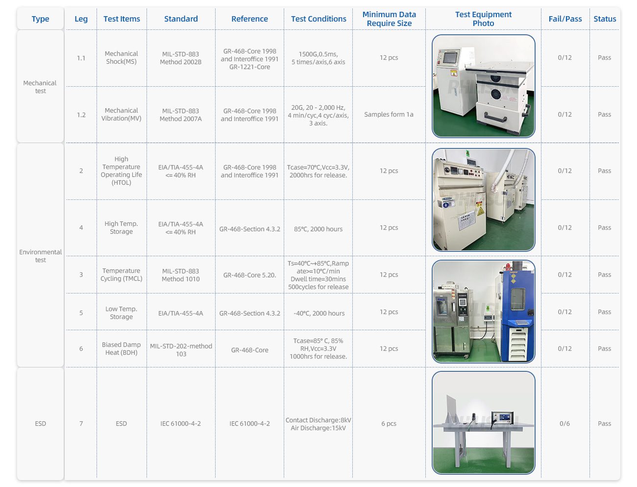
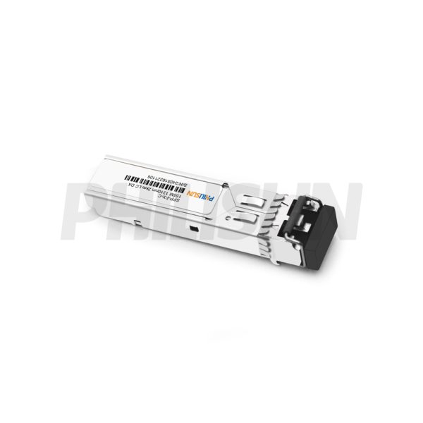
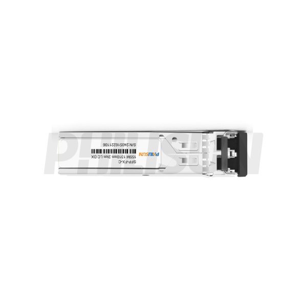
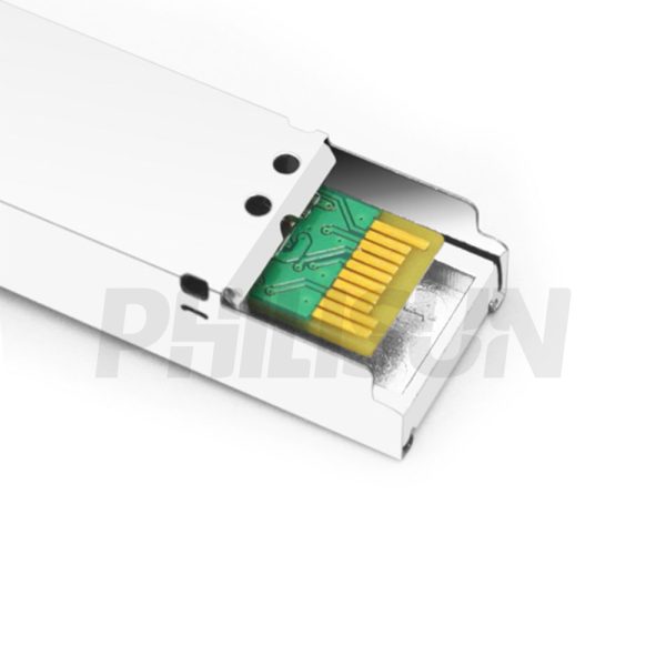
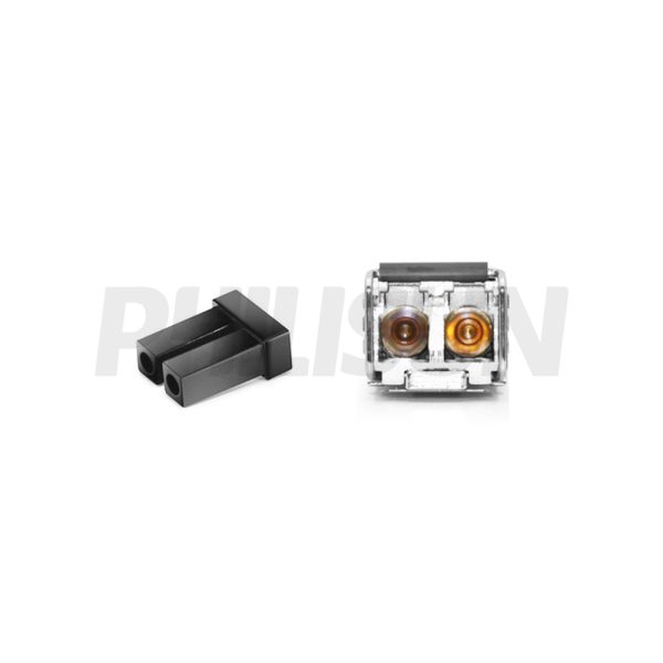
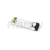
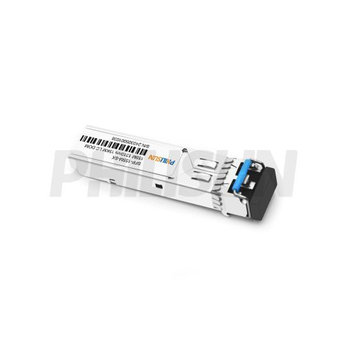
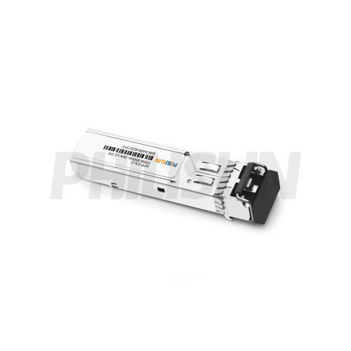
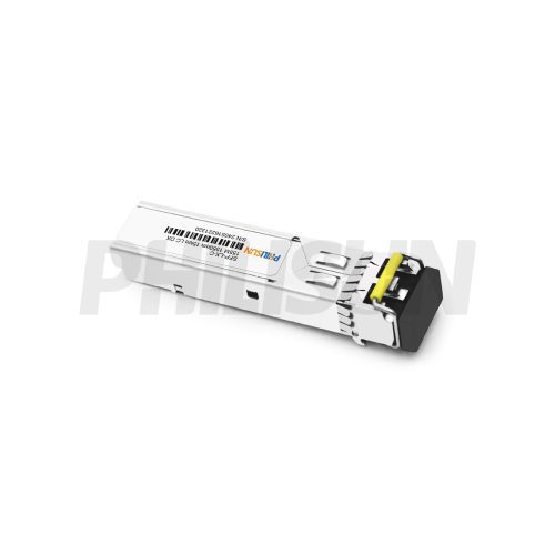
Generic Compatible 100BASE-FX SFP 1310nm 2km DOM Duplex LC MMF Optical Transceiver Module
SFP-0155-13-2-LCD-MM
- High Quality
- Factory Outlet
- Satisfaction Guarantee
- Global Shipping
| SPECIFICATIONS | |||
|---|---|---|---|
| Product Model | SFP-0155-13-2-LCD | Manufacturer Brand | PHILISUN |
| Package Type | SFP | Optical Connector | Duplex LC |
| Max Data Rate | ≤ 155Mbps | Channel Data Rate | - |
| Effective Transmission Distance | 2KM | ||
| Wavelength | 1310nm | Operating Voltage | 3.3V |
| Fiber Type | MMF | Core Size | 50/125 62.5/125 |
| Transmitter Type | FP | Receiver Type | IDP |
| TX Power | -19~-14dbm | Receiver Sensitivity | -31dBm |
| Digital Diagnostic Monitoring(DDM) | YES | Receiver Overload | -12dBm |
| Power Consumption | <1W | Protocols | SFP MSA SFF-8472 |
| Operating temperature(Commercial) | 0℃~+70℃ | Storage Temperature(Commercial) | -40℃~+85℃ |
| Operating temperature(Industrial) | -40℃~+85℃ | Storage Temperature(Industrial) | -40℃~+85℃ |


| Absolute Maximum Ratings | |||||||||
| Parameter | Symbol | Min. | Max. | Unit | |||||
| Storage temperature | TS | -4.0 | +85 | ℃ | |||||
| Supply voltage | VCC | -0.5 | 3.6 | V | |||||
| Operating relative humidity | – | – | 95 | % | |||||
| Exceeding any one of these values may destroy the device immediately | |||||||||
| Recommended Operating Environment | |||||||||
| Parameter | Symbol | Min | Typical | Max | Unit | ||||
| Operating case temperature | Tc | SFP-0155-13-2-LCD | 0 | – | +70 | °C | |||
| -40 | – | +85 | |||||||
| Power supply voltage | Vcc | 3.15 | 3.3 | 3.45 | V | ||||
| Power supply current | Icc | – | – | 300 | mA | ||||
| Date rate | OC-3/STM-1 | – | – | 155 | – | Mbps | |||
| 100M | – | – | 100 | – | |||||
| Performance Specifications – Electrical | |||||||||
| Parameter | Symbol | Min. | Typ. | Max. | Unit | Notes | |||
| Transmitter | |||||||||
| LVPECL inputs(Differential) | Vin | 400 | – | 2000 | mVpp | AC coupled inputs | |||
| Input impedance (Differential) | Zin | 85 | 100 | 115 | ohm | Rin > 100 kohm @ DC | |||
| TX_disable | Disable | – | 2 | – | Vcc+0.3 | V | – | ||
| Enable | – | 0 | – | 0.8 | – | ||||
| TX_FAULT | Fault | – | 2 | – | Vcc+0.3 | V | – | ||
| Normal | – | 0 | – | 0.5 | – | ||||
| Receiver | |||||||||
| LVPECL outputs (Differential) | Vout | 400 | – | 2000 | mVpp | AC coupled output | |||
| Output impedance (Differential) | Zout | 85 | 100 | 115 | ohms | – | |||
| RX_LOS | LOS | – | 2 | – | Vcc+0.3 | V | – | ||
| Normal | – | 0 | – | 0.8 | V | – | |||
| MOD_DEF ( 0:2 ) | VoH | 2.5 | – | – | V | With serial ID | |||
| VoL | 0 | – | 0.5 | V | |||||
| Optical and Electrical Characteristics | |||||||||
| Parameter | Symbol | Min. | Typical | Max. | Unit | ||||
| 50µm core diameter MMF | L | – | 2 | – | km | ||||
| Data rate | – | – | 125 | – | Mbps | ||||
| Transmitter | |||||||||
| Center wavelength | λC | 830 | 850 | 860 | nm | ||||
| Spectral width (RMS) | Δλ | – | – | 0.85 | nm | ||||
| Average output power | Pout | -9.5 | – | -4 | dBm | ||||
| Extinction ratio | ER | 8.2 | – | – | dB | ||||
| Rise/Fall time(20%~80%) | tr/tf | – | – | 3 | ps | ||||
| Total jitter | TJ | – | – | 1 | UI | ||||
| Output optical eye | IEEE 802.3 compliant | ||||||||
| TX disable assert time | t_off | – | – | 10 | us | ||||
| Receiver | |||||||||
| Center wavelength | λC | 760 | – | 860 | nm | ||||
| Receiver sensitivity | Pmin | – | – | -18 | dBm | ||||
| Receiver overload | Pmax | -3 | – | – | dBm | ||||
| Return loss | – | 14 | – | – | dB | ||||
| LOS de-assert | LOSD | – | – | -19 | dBm | ||||
| LOS assert | LOSA | -45 | – | – | dBm | ||||
| LOS hysteresis | – | 0.5 | – | – | dB | ||||
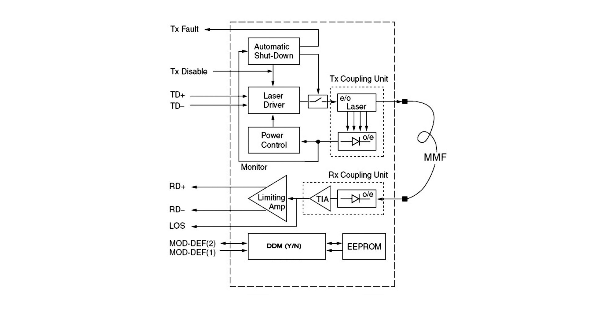
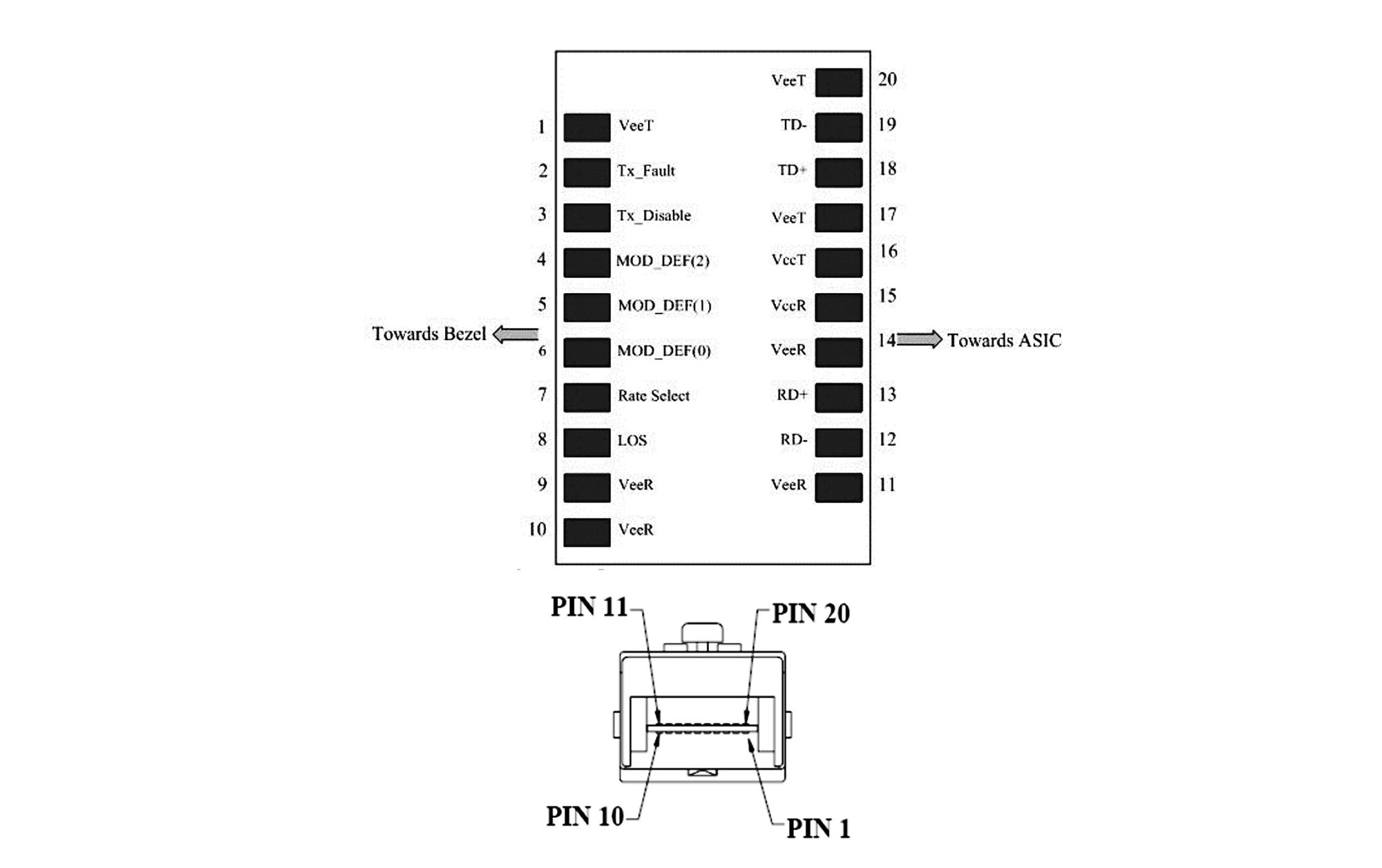
| Pin | Name | Function | Plug Seq. | Notes | |||||
| 1 | VeeT | Transmitter ground | 1 | – | |||||
| 2 | TX fault | Transmitter fault indication | 3 | 1) | |||||
| 3 | TX disable | Transmitter disable | 3 | 2) Module disables on high or open | |||||
| 4 | MOD-DEF2 | Module definition 2 | 3 | 3) Data line for serial ID. | |||||
| 5 | MOD-DEF1 | Module definition 1 | 3 | 3) Clock line for serial ID. | |||||
| 6 | MOD-DEF0 | Module definition 0 | 3 | 3) Grounded within the module. | |||||
| 7 | Rate select | Not connect | 3 | Function not available | |||||
| 8 | LOS | Loss of signal | 3 | 4) | |||||
| 9 | VeeR | Receiver ground | 1 | 5) | |||||
| 10 | VeeR | Receiver ground | 1 | 5) | |||||
| 11 | VeeR | Receiver ground | 1 | 5) | |||||
| 12 | RD- | Inv. received data out | 3 | 6) | |||||
| 13 | RD+ | Received data out | 3 | 6) | |||||
| 14 | VeeR | Receiver ground | 1 | 5) | |||||
| 15 | VccR | Receiver power | 2 | 7) 3.3V ± 5% | |||||
| 16 | VccT | Transmitter power | 2 | 7) 3.3V ± 5% | |||||
| 17 | VeeT | Transmitter ground | 1 | 5) | |||||
| 18 | TD+ | Transmit data In | 3 | 8) | |||||
| 19 | TD- | Inv. transmit data In | 3 | 8) | |||||
| 20 | VeeT | Transmitter ground | 1 | 5) | |||||
| Notes: 1) TX Fault is an open collector/drain output, which should be pulled up with a 4.7K – 10KΩ resistor on the host board. Pull up voltage between 2.0V and VccT/R+0.3V. When high, output indicates a laser fault of some kinds. Low indicates normal operation. In the low state, the output will be pulled to < 0.8V.2) TX disable is an input that is used to shutdown the transmitter optical output. It is pulled up within the module with a 4.7K – 10 KΩ resistor. Its states are: Low (0 – 0.8V): Transmitter on (>0.8, < 2.0V): Undefined High (2.0 – 3.465V): Transmitter Disabled Open: Transmitter Disabled3) Mod-Def 0,1,2. These are the module definition pins. They should be pulled up with a 4.7K – 10K resistor on the host board. The pull-up voltageshall be VccT or VccR . Mod-Def 0 is grounded by the module to indicate that the module is present Mod-Def 1 is the clock line of two wire serial interface for serial ID Mod-Def 2 is the data line of two wire serial interface for serial ID4) LOS is an open collector/drain output, which should be pulled up with a 4.7K – 10KΩ resistor. Pull up voltage between 2.0V and VccT/R+0.3V. When high, this output indicates the received optical power is below the worst-case receiver sensitivity (as defined by the standard in use).Low indicates normal operation. In the low state, the output will be pulled to < 0.8V. 5) VeeR and VeeT may be internally connected within the SFP module. 6) RD-/+: These are the differential receiver outputs. They are AC coupled 100Ω differential lines which should be terminated with 100Ω (differential) at the user SERDES. The AC coupling is done inside the module and is thus not required on the host board. The voltage swing on these lines will be between 400 and 2000 mV differential (200 –1000 mV single ended) when properly terminated. 7) VccR and VccT are the receiver and transmitter power supplies. They are defined as 3.3V ±5% at the SFP connector pin. Maximum supply current is 300Ma. Recommended host board power supply filtering is shown below. Inductors with DC resistance of less than 1ohm should be used in order to maintain the required voltage at the SFP input pin with 3.3V supply voltage. When the recommended supply-filtering network is used, hot plugging of the SFP transceiver module will result in an inrush current of no more than 30Ma greater than the steady state value.VccR and VccT may be internally connected within the SFP transceiver module. 8) TD-/+: These are the differential transmitter inputs. They are AC-coupled, differential lines with 100Ω differential termination inside the module. The AC coupling is done inside the module and is thus not required on the host board. The inputs will accept differential swings of 400 – 2000mV (200 – 1000mV single-ended). |
|||||||||

