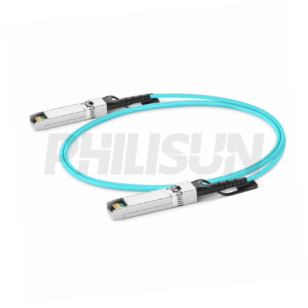
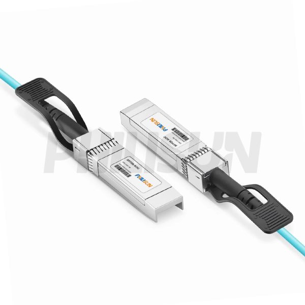
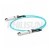
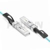
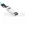
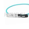
25G SFP28 to SFP28 Active Optical Cable (AOC)
Compliant with the SFF-8432 SFP28 MSA standard
Switch to Switch
Switch to GPU
Switch to Network Card
- High Quality
- Factory Outlet
- Satisfaction Guarantee
- Global Shipping
| SPECIFICATIONS | |||
|---|---|---|---|
| Cable End Connector A | SFP28 | Cable End Connector B | SFP28 |
| Jumper Type | Direct-Attach | Data Rate | 25G |
| Aggregate Bit Rate | 25.78125Gbps | Lane Bit Rate | 25Gbps |
| Number of Channels | 1 | Single Channel Rate | 25G |
| Array Transmitter | VSCEL | Array Receiver | PIN |
| Minimum Bend Radius | 30mm | Factory Brand | PHILISUN |
| Center(Operating) Wavelength | 850nm | Bit Error Rate | 10-15 |
| Fiber Type | OM3 MMF MAX 70m/OM4 MMF MAX 100m | Cable Colour | Aqua |
| Cable Material | LSZH/OFNP | Cable Length Selection | 1-100meter |
| Safety Certification | TUV/UL/FDA | Application Scenarios | 10/25 Gigabit Ethernet (10/25GbE) |
| Protocols | SFF-8432/SFF-8472/SFP28 MSA | DDMI(Commercial) | YES |
| Supply Voltage | 3.3V | Power Dissipation | <1W |
| Operating Temperature | 0 to 70℃ (32 to 158℉) | Storage Temperature | -40 to 85℃ (-40to185℉) |
PRODUCT PRESENTATION
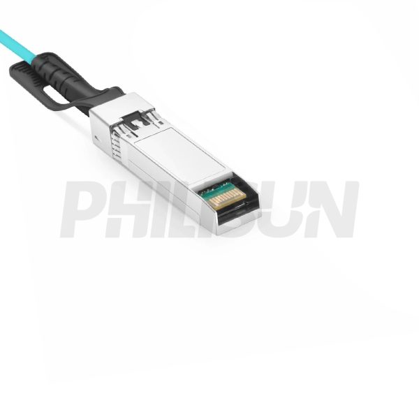
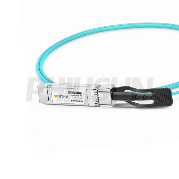
The PHILISUN SFP28(25G) Active Optical Cable is a direct-attach fiber assembly utilizing SFP28 connectors and the Multi-Mode Fiber (MMF) scheme. The product complies with the SFF-8431 MSA standard and is suitable for 25Gbps connections within racks and across adjacent racks. It uses OM3/OM4 Multimode Fiber. Its compact structure and fully sealed integrated optics reduce costs compared to conventional optical modules and jumpers, while significantly improving reliability and reducing maintenance. This AOC guarantees broad compatibility with major vendor platforms including Cisco, H3C, Huawei, Juniper, and Arista, and more.
AOC SERIES PRODUCTS
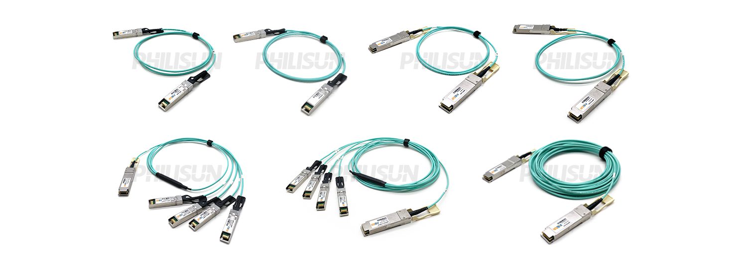
PRODUCTION & TESTING EQUIPMENT

PERFORMANCE PARAMETER
| Absolute Maximum Ratings | |||||||||
| Parameter | Symbol | Min | Typ. | Max | Unit | Ref. | |||
| Power Supply Voltage | VCC | 0 | – | 3.6 | V | – | |||
| Storage Temperature | Ts | 40 | – | 85 | ℃ | – | |||
| Operating Case Temperature | TC | 0 | – | 70 | ℃ | – | |||
| Relative Humidity | RH | 5 | – | 95 | % | – | |||
| Recommended Operating Conditions | |||||||||
| Parameter | Symbol | Min | Typ. | Max | Unit | Ref. | |||
| Power Supply Voltage | Vcc | 3.135 | 3.3 | 3.465 | V | – | |||
| Operating Case Temperature | TC | 0 | 25 | 70 | ℃ | – | |||
| Data Rate, each Lane | – | – | 25.78125 | – | Gb/s | – | |||
| Data Rate Accuracy | – | -100 | – | 100 | ppm | – | |||
| Control Input Voltage High | – | 2 | – | Vcc | V | – | |||
| Control Input Voltage Low | – | 0 | – | 0.8 | V | – | |||
| Fiber Bend Radius | Rbend | 3 | – | – | cm | – | |||
| Electrical Specifications | |||||||||
| Parameter | Symbol | Min | Typ. | Max | Unit | Ref. | |||
| Transmitter | |||||||||
| Power Consumption | – | – | – | 1 | W | 1 | |||
| Supply Current | Icc | – | – | 300 | mA | 1 | |||
| Overload Differential Voltage pk-pk | TP1a | – | – | – | mV | – | |||
| Common Mode Voltage (Vcm) | TP1 | -350 | – | 2850 | mV | 2 | |||
| Differential Termination Resistance Mismatch |
TP1 | – | – | 10 | % | At 1MHz | |||
| Differential Return Loss (SDD11) | TP1 | – | – | See CEI-28G VSR Equation 13-19 |
dB | – | |||
| Common Mode to Differential conversion and Differential to Common Mode conversion(SDC11, SCD11) |
TP1 | – | – | See CEI-28G VSR Equation 13-20 |
dB | – | |||
| Stressed Input Test | TP1a | – | – | See CEI 28G-VSR Section 13.3.11.2.1 |
– | – | |||
| Receiver | |||||||||
| Differential Voltage, pk-pk | TP4 | – | – | 900 | mV | – | |||
| Common Mode Voltage (Vcm) | TP4 | -350 | – | 2850 | mV | 2 | |||
| Common Mode Noise, RMS | TP4 | – | – | 17.5 | mV | At 1MHz | |||
| Differential Termination Resistance |
TP4 | – | – | 10 | % | – | |||
| Differential Return Loss (SDD22) | TP4 | – | – | See CEI-28G VSR Equation13- |
dB | – | |||
| Common Mode to Differential conversion and Differential to Common Mode conversion (SDC22, SCD22) |
TP4 | – | – | See CEI-28G VSR Equation13- 19 |
dB | – | |||
| Common Mode Return Loss(SCC22) | TP4 | – | – | -2 | dB | 3 | |||
| Transition Time, 20 to 80% | TP4 | – | – | – | Ps | – | |||
| Vertical Eye Closure (VEC) | TP4 | – | – | 5.5 | dB | – | |||
| Eye Width at 10-15 probability(EW15) | TP4 | 0.57 | – | – | UI | – | |||
| Eye Height at 10-15 probability(EH15) | TP4 | – | – | – | mV | – | |||
| Notes: 1.Per terminal. 2.Vcm is generated by the host. Specification includes effects of ground offset voltage. 3.From 250MHz to 30GHz . |
|||||||||
PIN ASSIGNMENT

Figure 1 – Interface to Host

Figure 2 – Contact Assignment
| Pin | Logic | Symbol | Description | Notes | |||||
| 1 | – | VeeT | Module Transmitter Ground | 1 | |||||
| 2 | LVTTL-O | TX_Fault | Module Transmitter Fault | – | |||||
| 3 | LVTTL-I | TX_Dis | Transmitter Disable; Turns off transmitter laser output | – | |||||
| 4 | LVTTL-I/O | SDA | 2-Wire Serial Interface Data Line | 2 | |||||
| 5 | LVTTL-I | SCL | 2-Wire Serial Interface Clock | 2 | |||||
| 6 | – | MOD-DEF0 | Module Definition, Grounded in the module | – | |||||
| 7 | LVTTL-I | RS0 | No connection required | – | |||||
| 8 | LVTTL-O | RX-LOS | Receiver Loss of Signal Indication. Logic 0 indicates normal operation | – | |||||
| 9 | LVTTL-I | RS1 | No connection required | – | |||||
| 10 | – | VeeR | Module Receiver Ground | 1 | |||||
| 11 | – | VeeR | Module Receiver Ground | 1 | |||||
| 12 | CML-O | RD- | Receiver Inverted Data Output | – | |||||
| 13 | CML-O | RD+ | Receiver Data Output | – | |||||
| 14 | – | VeeR | Module Receiver Ground | 1 | |||||
| 15 | – | VccR | Module Receiver 3.3 V Supply | – | |||||
| 16 | – | VccT | Module Receiver 3.3 V Supply | – | |||||
| 17 | – | VeeT | Module Transmitter Ground | 1 | |||||
| 18 | CML-I | TD+ | Transmitter Non-Inverted Data Input | – | |||||
| 19 | CML-I | TD- | Transmitter Inverted Data Input | – | |||||
| 20 | – | VeeT | Module Transmitter Ground | 1 | |||||
| Notes: 1. Module ground pins GND are isolated from the module case. 2. Shall be pulled up with 4.7K-10Kohms to a voltage between 3.15V and 3.45V on the host board. |
|||||||||
PRODUCT CERTIFICATION

COMPATIBLE BRANDS

CONFIGURATION INFORMATION


