

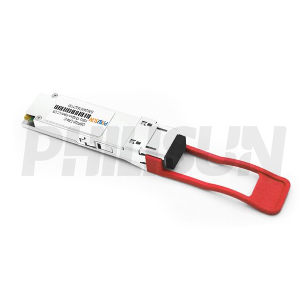
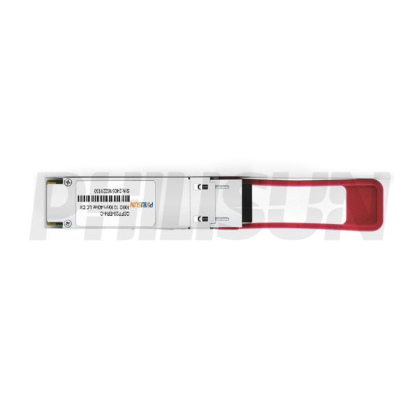

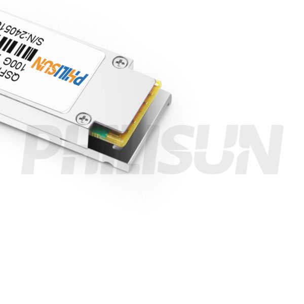
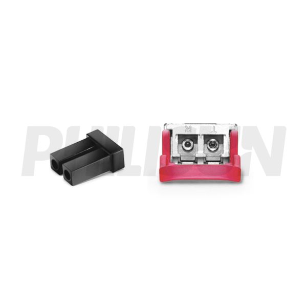
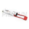
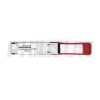

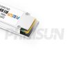
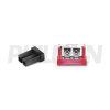
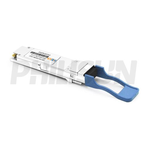
100G QSFP28 40km DOM Duplex LC SMF Optical Transceiver Module
QSFP28-103/112-LW-40(ER4)-LCD
- High Quality
- Factory Outlet
- Satisfaction Guarantee
- Global Shipping
| SPECIFICATIONS | |||
|---|---|---|---|
| Product Model | QSFP28-103/112-LW-40(ER4)-LCD | Manufacturer brand | PHILISUN |
| Package Type | QSFP28 | Optical connector | LC DX |
| Max Data Rate | 103.1Gbps | Channel Data Rate | 25.78125Gbps |
| Effective transmission distance | 40km | ||
| Wavelength | 1310nm | Operating voltage | 3.3V |
| Fiber Type | SMF | Core Size | 9/125 |
| Transmitter Type | DFB | Receiver Type | PIN |
| TX Power | -2.9~4.5dBm | Receiver Sensitivity | -18.6dBm |
| Digital Optical Monitoring(DOM) | YES | Receiver Overload | -4.9dBm |
| Power Consumption | <4.5W | Protocols | 100GBASE-ER4 Ethernet Links Infiniband QDR and DDR interconnects |
| Operating temperature(Commercial) | 0℃~+70℃ | Storage Temperature(Commercial) | -40℃~+85℃ |
PRODUCT PRESENTATION
The PHILISUN QSFP28 100G LAN-WDM 40km ER4 LC DX is a high-performance 100Gb/s transceiver module designed for optical communication applications compliant with the Ethernet 100GBASE-ER4 standard. It converts four 25Gb/s electrical input channels into four LAN WDM optical signals, multiplexing them into a single channel for 100Gb/s optical transmission. On the receiver side, it de-multiplexes the 100Gb/s optical input back into four LAN WDM optical signals and converts them into four electrical output channels.The central wavelengths of the four LAN WDM channels are 1295.56nm, 1300.05nm, 1304.58nm, and 1309.14nm, consistent with the LAN WDM wavelength grid defined in IEEE 802.3ba. Equipped with high-performance cooled LAN WDM DFB transmitters and high-sensitivity APD receivers, the module ensures exceptional performance for 100Gigabit Ethernet applications over links up to 40km.Designed according to the QSFP+ Multi-Source Agreement (MSA), the transceiver features a compact form factor, reliable optical/electrical connections, and a digital diagnostic interface. Built to withstand extreme operating conditions, including high temperatures, humidity, and EMI interference, it ensures robust and reliable performance in demanding environments.
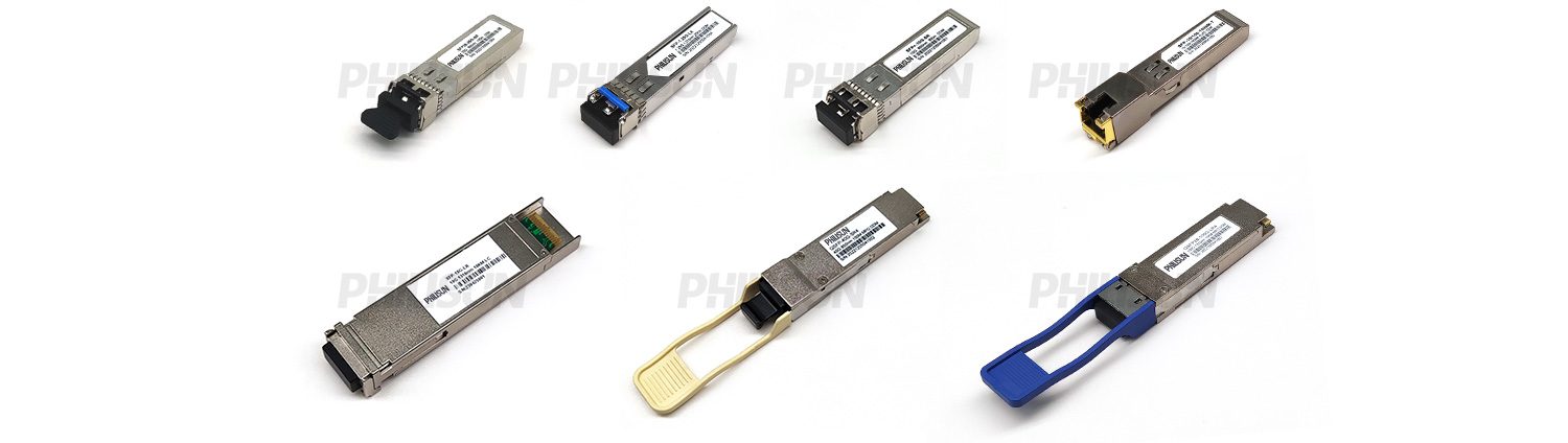
TRANSCEIVER SERIES PRODUCTS
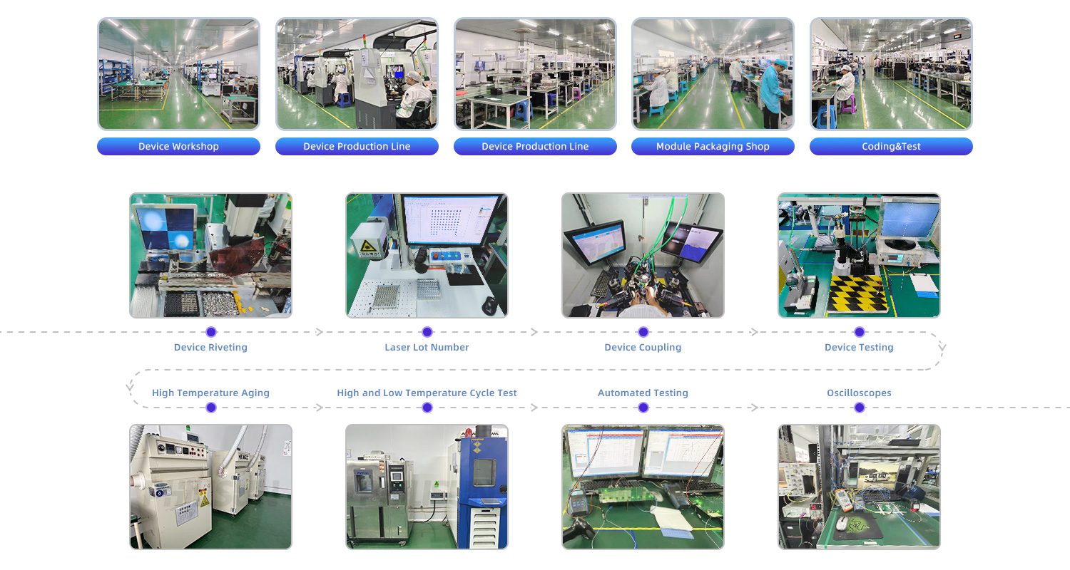
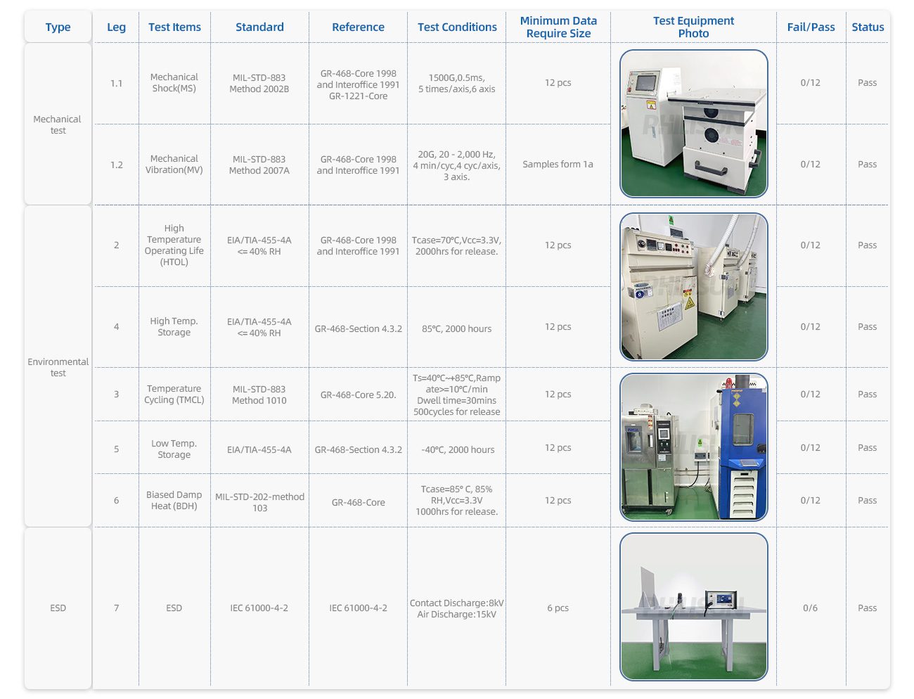
PRODUCTION & TESTING EQUIPMENT
PERFORMANCE PARAMETER
| Absolute Maximum Ratings | |||||||||
| Parameter | Symbol | Min. | Max. | Unit | |||||
| Supply voltage | VCC | -0.5 | +3.6 | V | |||||
| Storage temperature | TC | -20 | +85 | ℃ | |||||
| Relative humidity | RH | 5 | 85 | % | |||||
| These values represent the damage threshold of the module.Stress in excess of any of theindividual absolute maximum ratings can cause immediate catastrophic damage to the module even if all other parameters are within recommended operating conditions. | |||||||||
| Recommended Operating Environment | |||||||||
| Parameter | Symbol | Min | Typical | Max | Unit | ||||
| Power supply voltage | VCC | 3.13 | 3.3 | 3.47 | V | ||||
| Operating case temperature | Tca | 0 | – | 70 | ℃ | ||||
| Data rate per lane | fd | – | 25.78125 | – | Gb/s | ||||
| Link distance | D | – | – | 40 | km | ||||
| Electrical Characteristics | |||||||||
| Parameter | Symbol | Min | Typical | Max | Unit | Ref | |||
| Transmitter Section: | |||||||||
| Input differential impedance | Rin | 90 | 100 | 110 | Ω | 1 | |||
| Differential input voltage amplitude | Vin | 900 | – | – | mVp-p | 2 | |||
| Receiver | |||||||||
| Output differential impedance | Rout | 90 | 100 | 110 | Ω | 1 | |||
| Differential output voltage amplitude |
Vout | – | – | 900 | mVp-p | 3 | |||
| Notes: [1]AC coupled. [2]Differential input voltage amplitude is measuredbetween TxnP and TxnN. [3]Differentialoutput voltage amplitude is measured between RxnP and RxnN. |
|||||||||
| TransmitterSpecifications-Optical | |||||||||
| Parameter | Symbol | Min | Typical | Max | Unit | ||||
| Center wavelength | Ch0 | λ0 | 1294.53 | 1295.56 | 1296.59 | nm | |||
| Ch1 | λ1 | 1299.02 | 1300.05 | 1301.09 | nm | ||||
| Ch2 | λ2 | 1303.54 | 1304.58 | 1305.63 | nm | ||||
| Ch3 | λ3 | 1308.09 | 1309.14 | 1310.09 | nm | ||||
| Bit rate per channel | BR | 25.78125±100ppm | Gb/s | ||||||
| Side mode suppression ratio | SMSR | 30 | – | – | dB | ||||
| Average launch power,each lane | – | -2.9 | – | 4.5 | dBm | ||||
| Launch power in OMA minus TDP,each lane | OMA-TDP | -0.65 | – | – | dBm | ||||
| Transmission & dispersion penalty, each lane | TDP | – | – | 2.5 | dB | ||||
| Relative intensity noise | RIN | – | – | -130 | dB/Hz | ||||
| Transmitter reflectance | RT | – | – | -12 | dB | ||||
| Extinction ratio | ER | 7 | – | – | dB | ||||
| Transmitter eyemask definition {X1,X2,X3,Y1,Y2,Y3} |
{0.25,0.4,0.45,0.25,0.28,0.4} | ||||||||
| Average launch power of OFF transmitter,each lane | – | – | – | -30 | dBm | ||||
| Optical return loss tolerance | – | – | – | 20 | dB | ||||
| Receiver Specifications-Optical | |||||||||
| Parameter | Symbol | Min. | Typical | Max. | Unit | ||||
| Center wavelength | Ch0 | λ0 | 1294.53 | 1295.56 | 1296.59 | nm | |||
| Ch1 | λ1 | 1299.02 | 1300.05 | 1301.09 | nm | ||||
| Ch2 | λ2 | 1303.54 | 1304.58 | 1305.63 | nm | ||||
| Ch3 | λ3 | 1308.09 | 1309.14 | 1310.09 | nm | ||||
| Bit rate per channel | BR | 25.78125±100ppm | Gb/s | ||||||
| Damage threshold,each lane | – | – | – | -3 | dBm | ||||
| Averagereceive power,each lane | – | -20.9 | – | -4.9 | dbm | ||||
| Unstressed sensitivity(OMA) at 5×10⁵BER | OMA | – | – | -18.6 | dBm | ||||
| LOS assert | LOSA | -30 | – | – | dBm | ||||
| LOS de-assert | LOSD | – | – | -24 | dBm | ||||
QSFP28 TRANSCEIVER ELECTRICAL PAD LAYOUT
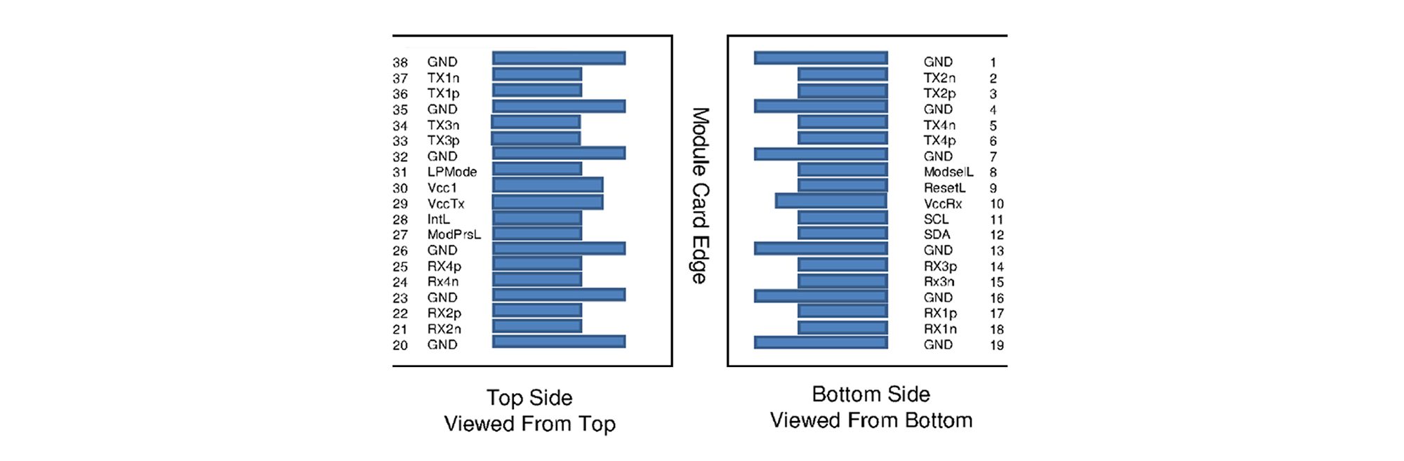
PIN DEFINITION
| Pin Definition | |||||||||
| Pin | Symbol | Name/Description | |||||||
| 1 | GND | Ground | |||||||
| 2 | Tx2n | Transmitter inverted data input | |||||||
| 3 | Tx2p | Transmitter non-inverted data input | |||||||
| 4 | GND | Ground | |||||||
| 5 | Tx4n | Transmitter inverted data input | |||||||
| 6 | Tx4p | Transmitter non-inverted data input | |||||||
| 7 | GND | Ground | |||||||
| 8 | ModSelL | Module select | |||||||
| 9 | ResetL | Module reset | |||||||
| 10 | VCCRx | +3.3V power supply receiver | |||||||
| 11 | SCL | 2-wire serial interface clock | |||||||
| 12 | SDA | 2-wire serial interface data | |||||||
| 13 | GND | Ground | |||||||
| 14 | Rx3p | Receiver non-inverted data output | |||||||
| 15 | Rx3n | Receiver inverted data output | |||||||
| 16 | GND | Ground | |||||||
| 17 | Rxlp | Receiver non-inverted data output | |||||||
| 18 | Rx1n | Receiver inverted data output | |||||||
| 19 | GND | Ground | |||||||
| 20 | GND | Ground | |||||||
| 21 | Rx2n | Receiver inverted data output | |||||||
| 22 | Rx2p | Receiver non-inverted data output | |||||||
| 23 | GND | Ground | |||||||
| 24 | Rx4n | Receiver inverted data output | |||||||
| 25 | Rx4p | Receiver non-inverted data output | |||||||
| 26 | GND | Ground | |||||||
| 27 | ModPrsL | Module present | |||||||
| 28 | IntL | Interrupt | |||||||
| 29 | VCCTx | +3.3V power supply transmitter | |||||||
| 30 | VCC1 | +3.3V power supply | |||||||
| 31 | LPMode | Low power mode | |||||||
| 32 | GND | Ground | |||||||
| 33 | Tx3p | Transmitter non-inverted data input | |||||||
| 34 | Tx3n | Transmitter inverted data input | |||||||
| 35 | GND | Ground | |||||||
| 36 | Txlp | Transmitter non-inverted data input | |||||||
| 37 | Tx1n | Transmitter inverted data input | |||||||
| 38 | GND | Ground | |||||||
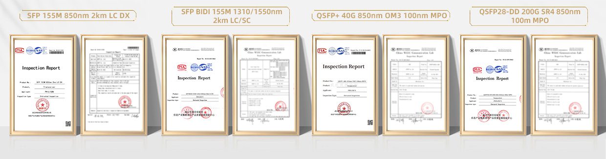
PRODUCT CERTIFICATION
QUALITY ADVANTAGE
COMPATIBLE BRANDS

CONFIGURATION INFORMATION
Related products
-
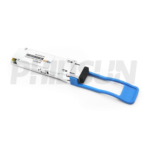
100G QSFP28 10km Breakout DOM Duplex LC SMF Optical Transceiver Module
QSFP28-103-LW-10(LR4)-LCD-OUT4
-
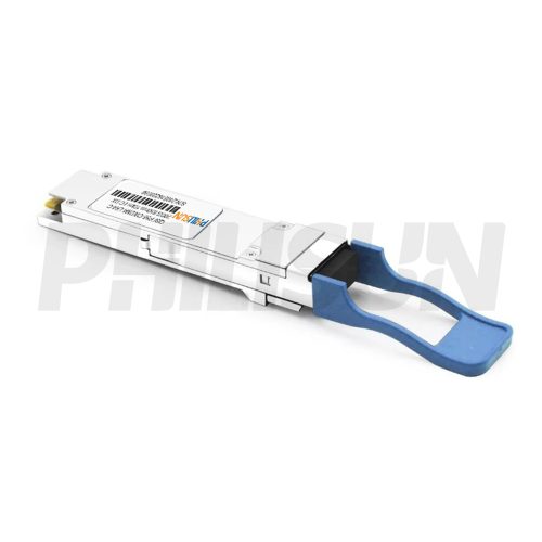
200G QSFP56 10km DOM Duplex LC SMF Optical Transceiver Module
QSFP56-200(4×50)-CW4-10(LR4)-LCD
-
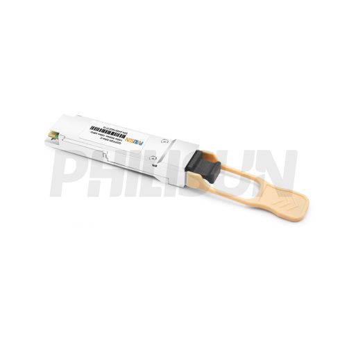
100GBASE-SR4 QSFP28 850nm 100m DOM MPO8/12 MMF Transceiver
QSFP28-103-85-01(SR4)-MPO8/12
-
200G QSFP56 2km DOM Duplex LC SMF Optical Transceiver Module
QSFP56-200(4×50)-CW4-2(FR4)-LCD