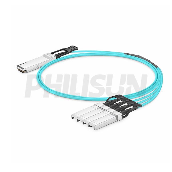
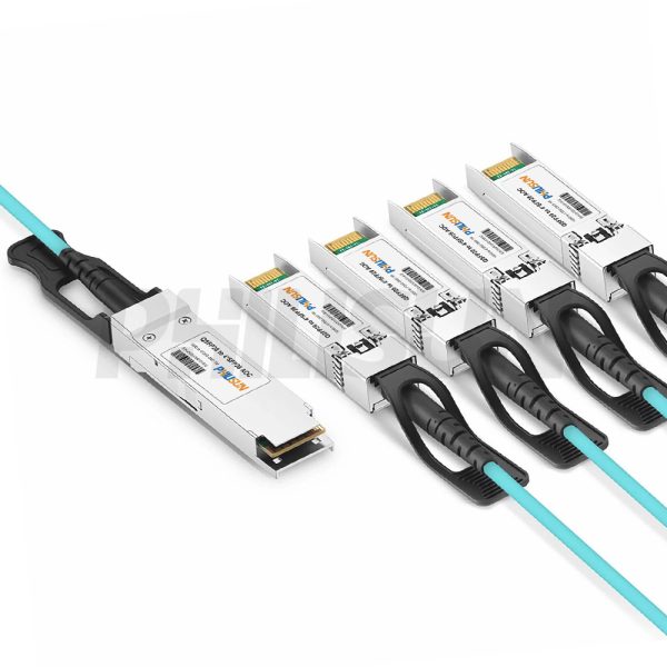
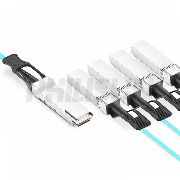
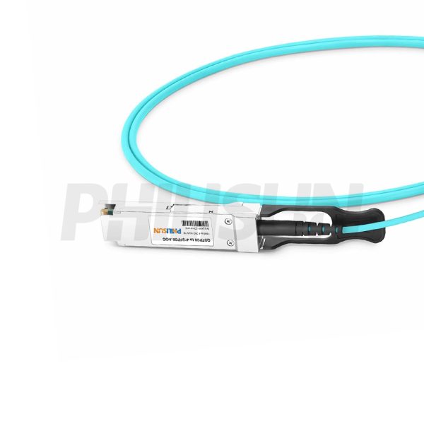
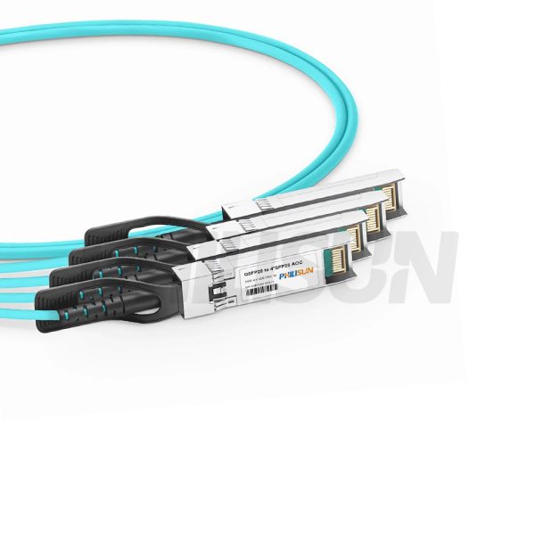
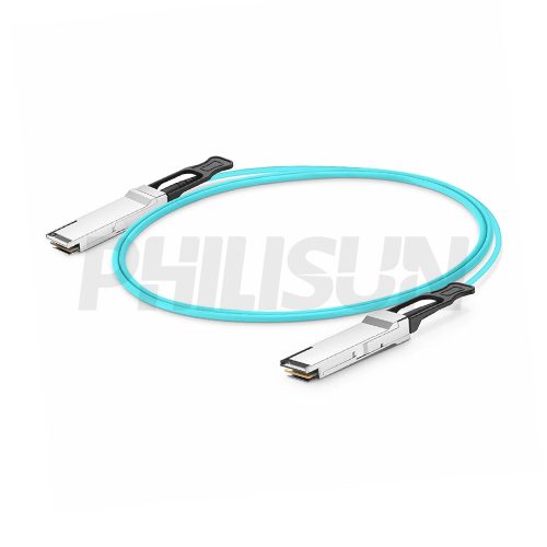
100G QSFP28 to 4×25G SFP28 Active Optical Cable(AOC)
Compliant with theSFF-8436 QSFP28 MSA standard
Switch to Switch
Switch to GPU
- High Quality
- Factory Outlet
- Satisfaction Guarantee
- Global Shipping
| SPECIFICATIONS | |||
|---|---|---|---|
| Cable End Connector A | QSFP28 | Cable End Connector B | 4×SFP28 |
| Jumper Type | Active Optical Breakout Cable | Data Rate | 100G |
| Aggregate Bit Rate | 103.125Gbps | Lane Bit Rate | 25.78125Gbps |
| Number of Channels | 4 | Single Channel Rate | 25G |
| Array Transmitter | VSCEL | Array Receiver | PIN |
| Minimum Bend Radius | 30mm | Factory Brand | PHILISUN |
| Center(Operating) Wavelength | 850nm | Bit Error Rate | 10-12 |
| Fiber Type | OM3 MMF MAX 70m/OM4 MMF MAX 100m | Cable Colour | Aqua |
| Cable Material | LSZH/OFNP | Cable Length Selection | 1-100meter |
| Safety Certification | TUV/UL/FDA | Application Scenarios | 100 /4x25 Gigabit Ethernet (100GbE) 100GBASE SR4/25GBASE SR Gigabit Ethernet |
| Protocols | SFF-8665/QSFP MSA/IEEE 802.3 bm | DDMI(Commercial) | YES |
| Supply Voltage | 3.3V | Power Dissipation | QSFP28: <3.5W SFP28: <1.0W |
| Operating Temperature | 0 to 70℃ (32 to 158℉) | Storage Temperature | -20 to 85℃ (-4 to 185℉) |
PRODUCT PRESENTATION
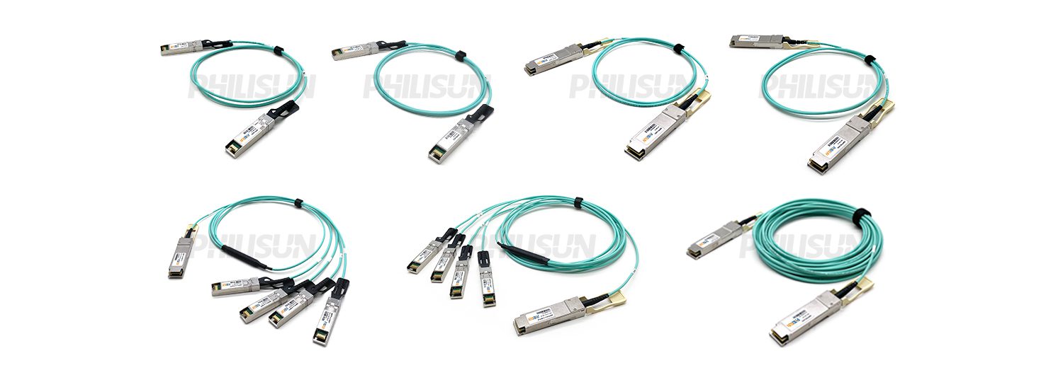
The PHILISUN 100G QSFP28 to 4×25G SFP28 Active Optical Breakout Cable is a direct-attach fiber assembly designed for linking 100G devices to 25G devices. The product complies with SFF-8436, SFF-8431, and MSA standards and is suitable for heterogeneous connections across adjacent racks. It uses OM3 Multimode Fiber. Its compact structure and fully sealed integrated optics reduce costs compared to conventional optical modules and jumpers, while significantly improving reliability and reducing maintenance. This AOC guarantees broad compatibility with major vendor platforms including Cisco, H3C, Huawei, Juniper, and Arista, and more.
AOC SERIES PRODUCTS
PRODUCTION & TESTING EQUIPMENT

PERFORMANCE PARAMETER
| Absolute Maximum Ratings | |||||||||
| Parameter | Symbol | Min | Typ. | Max | Unit | Ref. | |||
| Storage Temperature | Ts | -40 | – | 85 | ℃ | – | |||
| Operating Case Temperature | TOP | 0 | – | 70 | ℃ | – | |||
| Power Supply Voltage | VCC | -0.5 | – | 3.6 | V | – | |||
| Relative Humidity (non-condensation) | RH | 0 | – | 85 | % | – | |||
| Recommended Operating Environment | |||||||||
| Parameter | Symbol | Min | Typ. | Max | Unit | Ref. | |||
| Operating Case Temperature | TOP | 0 | – | 70 | ℃ | – | |||
| Power Supply Voltage | VCC | 3.135 | 3.3 | 3.465 | V | – | |||
| Data Rate, each Lane (QSFP28) | – | – | 25.78125 | – | Gb/s | – | |||
| Data Rate (each SFP28) | – | – | 25.78125 | – | Gb/s | – | |||
| Control Input Voltage High | – | 2 | – | VCC | V | – | |||
| Control Input Voltage Low | – | 0 | – | 0.8 | V | – | |||
| Electrical Characteristics-QSFP28 Terminal | |||||||||
| Parameter | Symbol | Min | Typ. | Max | Unit | Ref. | |||
| Power Consumption, each Terminal | – | – | – | 3.5 | W | – | |||
| Supply Current, each Terminal | Icc | – | – | 1060 | mA | – | |||
| Transceiver Power-on Initialization Time | – | – | – | 2000 | ms | 1 | |||
| Transmitter (each Lane) | |||||||||
| Single Ended Input Voltage Tolerance (Note 2) |
– | -0.3 | – | 3.6 | V | – | |||
| AC Common Mode Input Voltage Tolerance |
– | 15 | – | – | mV | RMS | |||
| Differential Input Voltage Swing Threshold | – | 50 | – | – | mVpp | LOSA Threshold |
|||
| Differential Input Voltage Swing | Vin,pp | 180 | – | 1000 | mVpp | – | |||
| Differential Input Impedance | Zin | 90 | 100 | 110 | Ohm | – | |||
| Total Jitter | – | – | – | 0.40 | UI | – | |||
| Deterministic Jitter | – | – | – | 0.15 | UI | – | |||
| Receiver (each Lane) | |||||||||
| Single Ended Output Voltage | – | -0.3 | – | 4 | V | – | |||
| AC Common Mode Output Voltage | – | – | – | 7.5 | mV | RMS | |||
| Differential Output Voltage Swing | Vout,pp | 300 | – | 1000 | mVpp | – | |||
| Differential Output Impedance | Zout | 90 | 100 | 110 | Ohm | – | |||
| Total Jitter | – | – | – | 0.3 | UI | – | |||
| Deterministic Jitter | – | – | – | 0.15 | UI | – | |||
| Electrical Characteristics-SFP28 Terminal | |||||||||
| Parameter | Symbol | Min | Typ. | Max | Unit | Ref. | |||
| Power Consumption | – | – | 1000 | mW | – | ||||
| Supply Current, each SFP28 | Icc | – | – | 300 | mA | – | |||
| Transceiver Power-on Initialization Time | – | – | – | 300 | ms | 1 | |||
| Transmitter | |||||||||
| Single Ended Input Voltage Tolerance | – | -0.3 | – | 4 | V | – | |||
| AC Common Mode Voltage Tolerance | – | 15 | – | – | mV | RMS | |||
| Differential Input Voltage Swing | Vin,pp | 180 | – | 700 | mV | – | |||
| Differential Input Impedance | Zin | 90 | 100 | 110 | Ohm | – | |||
| Data Dependent Input Jitter | DDJ | – | – | 0.40 | UI | – | |||
| Data Input Total Jitter | TJ | – | – | 0.15 | UI | – | |||
| Receiver | |||||||||
| Single Ended Output Voltage | – | -0.3 | – | 4 | V | – | |||
| AC Common Mode Voltage | – | – | – | 7.5 | mV | RMS | |||
| Differential Output Voltage Swing | Vout,pp | 300 | – | 850 | mVpp | – | |||
| Differential Output Impedance | Zout | 90 | 100 | 110 | Ohm | – | |||
| Rx Output Rise and Fall Time | Tr/Tf | 30 | – | – | ps | 20% to 80% | |||
| Total Jitter | TJ | – | – | 0.3 | UI | – | |||
| Deterministic Jitter | DJ | – | – | 0.15 | UI | – | |||
PIN ASSIGNMENT-QSFP28 TERMINAL
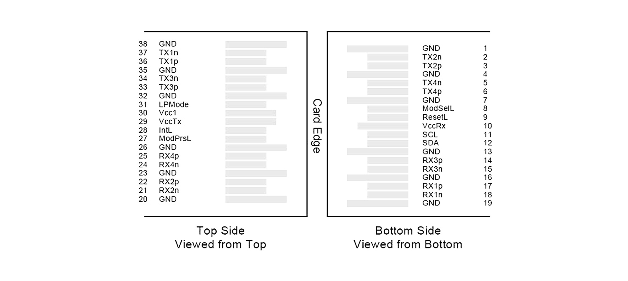
Figure 1 – MSA compliant QSFP28 Connector
| Pin | Logic | Symbol | Description | Notes | |||||
| 1 | – | GND | Ground | 1 | |||||
| 2 | CML-I | Tx2n | Transmitter Inverted Data Input | – | |||||
| 3 | CML-I | Tx2p | Transmitter Non-Inverted Data output | – | |||||
| 4 | – | GND | Ground | 1 | |||||
| 5 | CML-I | Tx4n | Transmitter Inverted Data Input | – | |||||
| 6 | CML-I | Tx4p | Transmitter Non-Inverted Data output | – | |||||
| 7 | – | GND | Ground | 1 | |||||
| 8 | LVTLL-I | ModSelL | Module Select | – | |||||
| 9 | LVTLL-I | ResetL | Module Reset | – | |||||
| 10 | – | VccRx | +3.3 V Power Supply Receiver | 2 | |||||
| 11 | LVCMOS-I/O | SCL | 2-wire serial interface clock | – | |||||
| 12 | LVCMOS-I/O | SDA | 2-wire serial interface data | – | |||||
| 13 | – | GND | Ground | – | |||||
| 14 | CML-O | Rx3p | Receiver Non-Inverted Data Output | – | |||||
| 15 | CML-O | Rx3n | Receiver Inverted Data Output | – | |||||
| 16 | – | GND | Ground | 1 | |||||
| 17 | CML-O | Rx1p | Receiver Non-Inverted Data Output | – | |||||
| 18 | CML-O | Rx1n | Receiver Inverted Data Output | – | |||||
| 19 | – | GND | Ground | 1 | |||||
| 20 | – | GND | Ground | 1 | |||||
| 21 | CML-O | Rx2n | Receiver Inverted Data Output | – | |||||
| 22 | CML-O | Rx2p | Receiver Non-Inverted Data Output | – | |||||
| 23 | – | GND | Ground | 1 | |||||
| 24 | CML-O | Rx4n | Receiver Inverted Data Output | 1 | |||||
| 25 | CML-O | Rx4p | Receiver Non-Inverted Data Output | – | |||||
| 26 | – | GND | Ground | 1 | |||||
| 27 | LVTTL-O | ModPrsL | Module Present | – | |||||
| 28 | LVTTL-O | IntL | Interrupt | – | |||||
| 29 | – | VccTx | +3.3V Power supply transmitter | 2 | |||||
| 30 | – | Vcc1 | +3.3V Power supply | 2 | |||||
| 31 | LVTTL-I | LPMode | Low Power Mode | – | |||||
| 32 | – | GND | Ground | 1 | |||||
| 33 | CML-I | Tx3p | Transmitter Non-Inverted Data Input | – | |||||
| 34 | CML-I | Tx3n | Transmitter Inverted Data Output | – | |||||
| 35 | – | GND | Ground | 1 | |||||
| 36 | CML-I | Tx1p | Transmitter Non-Inverted Data Input | – | |||||
| 37 | CML-I | Tx1n | Transmitter Inverted Data Output | – | |||||
| 38 | – | GND | Ground | 1 | |||||
| Notes: 1.GND is the symbol for signal and supply (power) common for QSFP28 modules. All are common within the QSFP28 module and all module voltages are referenced to this potential unless otherwisenoted.Connectthesedirectlytothehostboardsignalcommongroundplane.2.VccRx, Vcc1 and VccTx are the receiving and transmission power suppliers and shall be applied concurrently. Recommended host board power supply filtering is shown in Figure 4 below. Vcc Rx, Vcc1 and VccTx may be internally connected within the QSFP28 transceiver module in any combination. The connector pins are each rated for a maximum current of 1000mA. |
|||||||||
PIN ASSIGNMENT-SFP28 TERMINAL
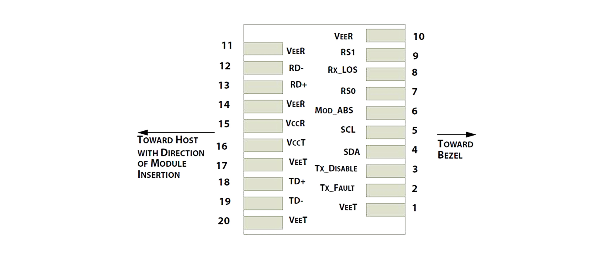
Figure 2 – SFP28 Module Interface to Host
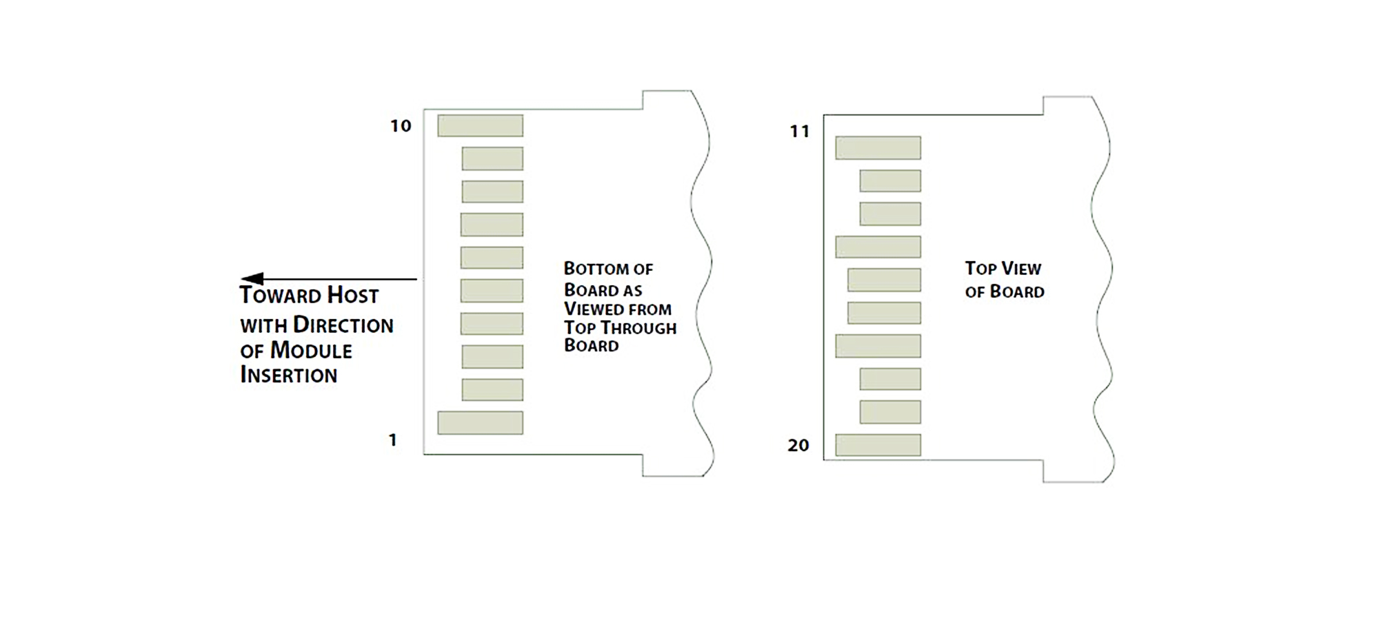
Figure 3 – SFP28 Module Contact Assignment
| Pin | Logic | Symbol | Description | Notes | |||||
| 1 | – | VeeT | Module Transmitter Ground | 1 | |||||
| 2 | LVTTL-O | TX_Fault | Module Transmitter Fault | – | |||||
| 3 | LVTTL-I | TX_Dis | Transmitter Disable; Turns off transmitter laser output | – | |||||
| 4 | LVTTL-I/O | SDA | 2-Wire Serial Interface Data Line | 2 | |||||
| 5 | LVTTL-I | SCL | 2-Wire Serial Interface Clock | 2 | |||||
| 6 | – | MOD-DEF0 | Module Definition, Grounded in the module | – | |||||
| 7 | LVTTL-I | RS0 | Receiver Rate Select | – | |||||
| 8 | LVTTL-O | RX-LOS | Receiver Loss of Signal Indication Active LOW | – | |||||
| 9 | LVTTL-I | RS1 | Transmitter Rate Select (not used) | – | |||||
| 10 | – | VeeR | Module Receiver Ground | 1 | |||||
| 11 | – | VeeR | Module Receiver Ground | 1 | |||||
| 12 | CML-O | RD- | Receiver Inverted Data Output | – | |||||
| 13 | CML-O | RD+ | Receiver Data Output | – | |||||
| 14 | – | VeeR | Module Receiver Ground | 1 | |||||
| 15 | – | VccR | Module Receiver 3.3 V Supply | – | |||||
| 16 | – | VccT | Module Receiver 3.3 V Supply | – | |||||
| 17 | – | VeeT | Module Transmitter Ground | 1 | |||||
| 18 | CML-I | TD+ | Transmitter Non-Inverted Data Input | – | |||||
| 19 | CML-I | TD- | Transmitter Inverted Data Input | – | |||||
| 20 | – | VeeT | Module Transmitter Ground | 1 | |||||
| Notes: 1. Module ground pins GND are isolated from the module case. 2. Shall be pulled up with 4.7K-10Kohms to a voltage between 3.15V and 3.45V on the host board. |
|||||||||
PRODUCT CERTIFICATION

COMPATIBLE BRANDS

CONFIGURATION INFORMATION


