

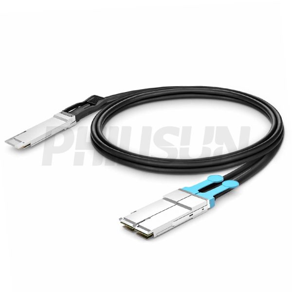
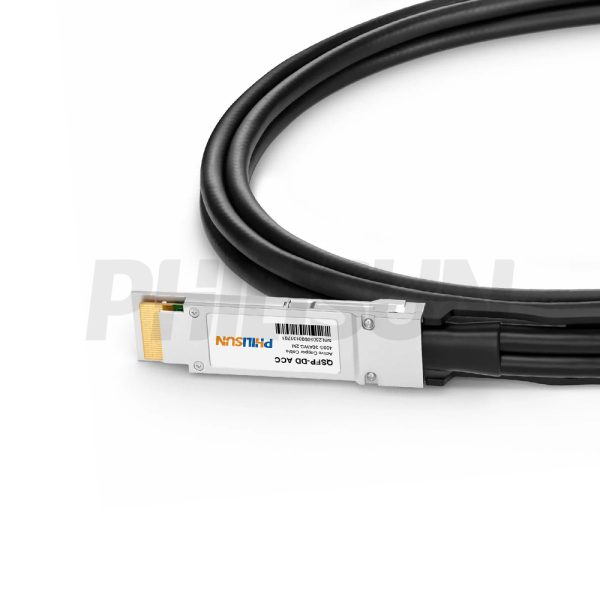


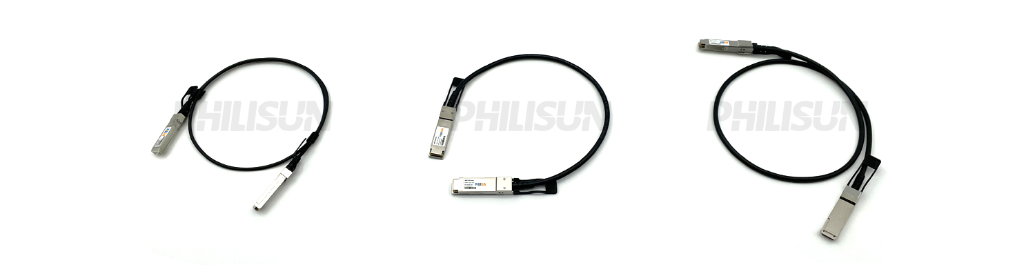
400G QSFP-DD to 2×200G QSFP56 ACC
Compliant with
QSFP-DD MSA, SFF-8636 standard
Switch to Switch
Switch to GPU
- High Quality
- Factory Outlet
- Satisfaction Guarantee
- Global Shipping
| SPECIFICATIONS | |||
|---|---|---|---|
| Cable End Connector A | QSFP-DD | Cable End Connector B | 2×QSFP56 |
| Jumper Type | Active Optical Breakout Cable | Data Rate | 400G |
| Aggregate Bit Rate | 425Gbps | Lane Bit Rate | 53.125Gbps |
| Number of Channels | 8 | Single Channel Rate | 50G |
| Minimum Bend Radius | 5X Cable OD -Single, 10X Cable OD - Repeated | Factory Brand | PHILISUN |
| Attenuation | 26AWG:10dB/8.5m maximum 28AWG:10dB/7m maximum 30AWG:8.4dB/5.5m maximum | Bit Error Rate | ≤10-12 |
| Shield | Braid/Foil | Wire AWG | 26AWG/28AWG/30AWG |
| Cable Type | Active Twinax | Cable OD | 30AWG: 14.0mm 28AWG:16.0mm 26AWG:18.0mm |
| Cable Colour/Material | Black PVC(OFNR) | Cable Length Selection | 1-7meter |
| Protocols | QSFP-DD MSA/SFF-8636/SFF-8679 | Application Scenarios | 400Gigabit Ethernet (400GbE) |
| Supply Voltage | 3.3V | Power Dissipation | <3.0W |
| Operating Temperature | 0 to 70℃ (32 to 158℉) | Storage Temperature | -40 to 85℃ (-40 to 185℉) |
PRODUCT PRESENTATION
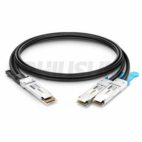
The PHILISUN 400G QSFP-DD to 2x200G QSFP56 high-speed breakout cable assembly is designed for high-density standard and composite connector configurations.This QSFP-DD pluggable solution supports 400G transmission and is fully compliant with QSFP-DD MSA, SFF-8636 and SFF-8679 standards.It delivers a high-performance, high-bandwidth, cost-effective interconnect solution supporting 400G applications across various rates.
DAC SERIES PRODUCTS
PRODUCTION & TESTING EQUIPMENT

PERFORMANCE PARAMETER
| Absolute Maximum Ratings | |||||||||
| Parameter | Min. | Max. | Unit | ||||||
| Storage Temperature | -45 | 80 | ℃ | ||||||
| Operating Relative Humidity | – | 85 | % | ||||||
| Power Supply not Damaged Voltage | -0.5 | 3.6 | V | ||||||
| Recommended Operating Conditions | |||||||||
| Parameter | Min. | Typ. | Max. | Unit | |||||
| Operating Case Temperature | 0 | – | 70 | ℃ | |||||
| Power Supply Working Voltage | 3.135 | 3.3 | 3.65 | V | |||||
| Bit Rat | – | 400 | – | Gbps | |||||
| Characteristics | |||||||||
| All performance is defined over the recommended operating environment unless otherwise specified. | |||||||||
| Item | arameter | Reference | |||||||
| SDD21 | 8dB<X<17.16dB @13.28 GHz | IEEE802.3cd, Clause136.11.2 | |||||||
| SDD11/22 | ‘-16.5+2*sqrt(f)dB Max @0.05GHz- 4.1GHz -10.66+14*1og(f/5.5) dB Max@4.1GHz-19GHz |
– | |||||||
| SCD11/22 | – | IEEE802.3cd, Clause 136.11.4 | |||||||
| SCD21-SDD21 | -10dB Max @0.01GHz~12.89GHz -27+(29/22) *f dB Max @12.89GHz~15.7GHz -6.3dB Max. @15.7GHz~19GHz |
IEEE802.3cd, Clause 136.11.5 | |||||||
| SCC11/22 | -2dB Max. @0.2GHz~19GHz | IEEE802.3cd, Clause 136.11.6 | |||||||
| COM | 3 dB MindB | – | |||||||
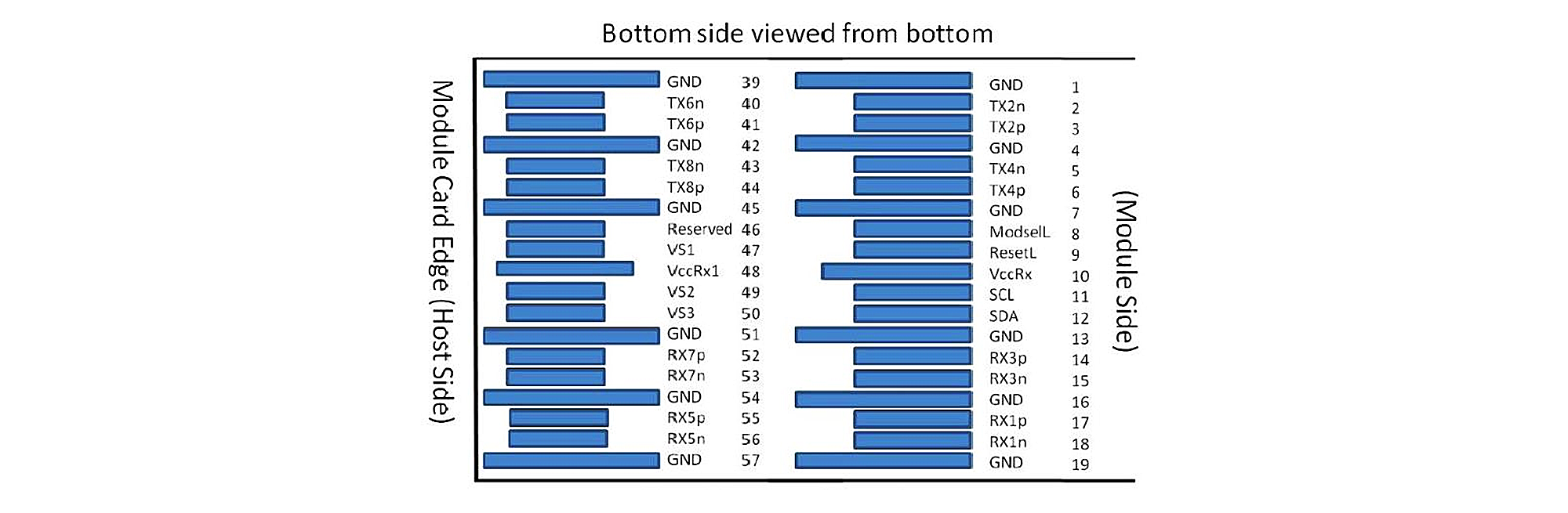
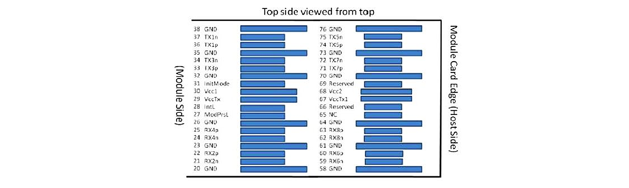
| PIN Function Definitions of QSFP-DD | |||||||||
| Noz | Symbol | Level / Logic | Description | ||||||
| 1 | GND | – | Module Ground | ||||||
| 2 | Tx2n | CML-I | Transmitter Inverted Data Input | ||||||
| 3 | Tx2p | CML-I | Transmitter Non-Inverted Data Input | ||||||
| 4 | GND | – | Module Ground | ||||||
| 5 | Tx4n | CML-I | Transmitter Inverted Data Input | ||||||
| 6 | Tx4p | CML-I | Transmitter Non-Inverted Data InputPin | ||||||
| 7 | GND | – | Module Ground | ||||||
| 8 | ModSelL | LVTTL-I | Module Select | ||||||
| 9 | ResetL | LVTTL-I | Module Reset | ||||||
| 10 | VccRx | – | +3.3V Power Supply for Receiver | ||||||
| 11 | SCL | LVTTL-I | 2-Wire Serial Interface Clock | ||||||
| 12 | SDA | LVTTL-I/O | 2-Wire Serial Interface Data Line | ||||||
| 13 | GND | – | Module Ground | ||||||
| 14 | Rx3p | CML-O | Receiver Non-Inverted Data Output | ||||||
| 15 | RX3n | CML-O | Receiver Inverted Data output | ||||||
| 16 | GND | – | Module Ground | ||||||
| 17 | Rx1p | CML-O | Receiver Non-Inverted Data Output | ||||||
| 18 | Rx1n | CML-O | Receiver Inverted Data Output | ||||||
| 19 | GND | – | Module Ground | ||||||
| 20 | GND | – | Module Ground | ||||||
| 28 | IntL/RxLOSL | LVTTL-O | Interrupt. Optionally configurable as RxLOSL via the management interface (SFF-8636). |
||||||
| 29 | VccTx | – | +3.3V Power Supply for Transmitter | ||||||
| 30 | Vcc1 | – | +3.3V Power Supply | ||||||
| 31 | LPMode/TxDis | LVTTL-I | Low Power Mode. Optionally configurable as TxDis via the management interface (SFF-8636). |
||||||
| 32 | GND | – | Module Ground | ||||||
| 33 | Tx3p | CML-I | Transmitter Non-Inverted Data Input | ||||||
| 34 | Tx3n | CML-I | Transmitter Inverted Data Input | ||||||
| 35 | GND | – | Module Ground | ||||||
| 36 | Tx1p | CML-I | Transmitter Non-Inverted Data Input | ||||||
| 37 | Tx1n | CML-I | Transmitter Inverted Data Input | ||||||
| 38 | GND | – | Module Ground | ||||||
| 39 | GND | – | Module Ground | ||||||
| 40 | Tx6n | CML-I | Transmitter Inverted Data Input | ||||||
| 41 | Tx6p | CML-I | Transmitter Non-Inverted Data Input | ||||||
| 42 | GND | – | Module Ground | ||||||
| 43 | Tx8n | CML-I | Transmitter Inverted Data Input | ||||||
| 44 | Tx8p | CML-I | Transmitter Non-Inverted Data Input | ||||||
| 45 | GND | – | Module Ground | ||||||
| 46 | Reserved | – | For future use | ||||||
| 47 | VSI | – | Module Vendor Specific 1 | ||||||
| 48 | VccRx1 | – | 3.3V Power Supply | ||||||
| 49 | VS2 | – | Module Vendor Specific 2 | ||||||
| 50 | VS3 | – | Module Vendor Specific 3 | ||||||
| 51 | GND | – | Module Ground | ||||||
| 52 | Rx7p | CML-O | Receiver Non-Inverted Data Output | ||||||
| 53 | Rx7n | CML-O | Receiver Inverted Data Output | ||||||
| 54 | GND | – | Module Ground | ||||||
| 55 | Rx5p | CML-O | Receiver Non-Inverted Data Output | ||||||
| 56 | Rx5n | CML-O | Receiver Inverted Data Output | ||||||
| 57 | GND | – | Module Ground | ||||||
| 58 | GND | – | Module Ground | ||||||
| 59 | Rx6n | CML-O | Receiver Inverted Data Output | ||||||
| 60 | Rx6p | CML-O | Receiver Non-Inverted Data Output | ||||||
| 61 | GND | – | Module Ground | ||||||
| 62 | Rx8n | CML-O | Receiver Inverted Data Output | ||||||
| 63 | Rx8p | CML-O | Receiver Non-Inverted Data Output | ||||||
| 64 | GND | – | Module Ground | ||||||
| 65 | NC | – | No Connect | ||||||
| 66 | Reserved | – | For future use | ||||||
| 67 | VccTx1 | – | 3.3V Power Supply | ||||||
| 68 | Vcc2 | – | 3.3V Power Supply | ||||||
| 69 | Reserved | – | For future use | ||||||
| 70 | GND | – | Module Ground | ||||||
| 71 | Tx7p | CML-I | Transmitter Non-Inverted Data Input | ||||||
| 72 | Tx7n | CML-I | Transmitter Inverted Data Input | ||||||
| 73 | GND | – | Module Ground | ||||||
| 74 | Tx5p | CML-I | Transmitter Non-Inverted Data Input | ||||||
| 75 | Tx5n | CML-I | Transmitter Inverted Data Input | ||||||
| 76 | GND | – | Module Ground | ||||||
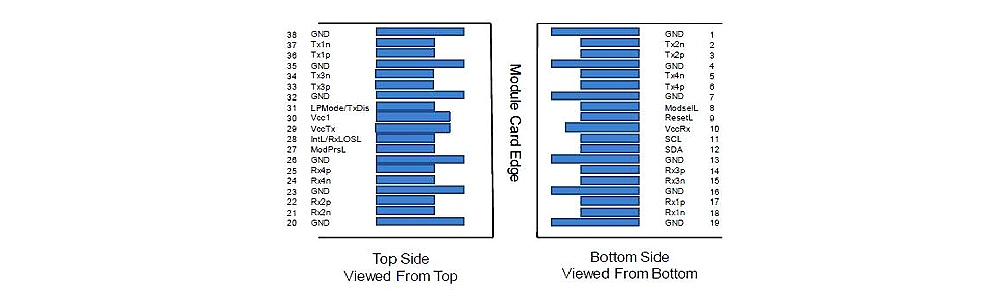
| PIN Function Definitions of QSFP56 | |||||||||
| Pin No. | Symbol | Level / Logic | Description | ||||||
| 1 | GND | – | Module Ground | ||||||
| 2 | Tx2n | CML-I | Transmitter Inverted Data Input | ||||||
| 3 | Tx2p | CML-I | Transmitter Non-Inverted Data Input | ||||||
| 4 | GND | – | Module Ground | ||||||
| 5 | Tx4n | CML-I | Transmitter Inverted Data Input | ||||||
| 6 | Tx4p | CML-I | Transmitter Non-Inverted Data Input | ||||||
| 7 | GND | – | Module Ground | ||||||
| 8 | ModSelL | LVTTL-I | Module Select | ||||||
| 9 | ResetL | LVTTL-I | Module Reset | ||||||
| 10 | VccRx | – | +3.3V Power Supply for Receiver | ||||||
| 11 | SCL | LVTTL-I | 2-Wire Serial Interface Clock | ||||||
| 12 | SDA | LVTTL-I/O | 2-Wire Serial Interface Data Line | ||||||
| 13 | GND | – | Module Ground | ||||||
| 14 | Rx3p | CML-O | Receiver Non-Inverted Data Output | ||||||
| 15 | Rx3n | CML-O | Receiver Inverted Data Output | ||||||
| 16 | GND | – | Module Ground | ||||||
| 17 | Rx1p | CML-O | Receiver Non-Inverted Data Output | ||||||
| 18 | Rx1n | CML-O | Receiver Inverted Data Output | ||||||
| 19 | GND | – | Module Ground | ||||||
| 20 | GND | – | Module Ground | ||||||
| 21 | Rx2n | CML-O | Receiver Inverted Data Output | ||||||
| 22 | Rx2p | CML-O | Receiver Non-Inverted Data Output | ||||||
| 23 | GND | – | Module Ground | ||||||
| 24 | Rx4n | CML-O | Receiver Inverted Data Output | ||||||
| 25 | Rx4p | CML-O | Receiver Non-Inverted Data Output | ||||||
| 26 | GND | – | Module Ground | ||||||
| 27 | ModPrsL | LVTTL-O | Module Present | ||||||
| 28 | IntL/RxLOSL | LVTTL-O | Interrupt. Optionally configurable as RxLOSL via the management interface (SFF-8636). |
||||||
| 29 | VccTx | – | +3.3V Power Supply for Transmitter | ||||||
| 30 | Vcc1 | – | +3.3V Power Supply | ||||||
| 31 | LPMode/TxDis | LVTTL-I | Low Power Mode. Optionally configurable as TxDis via the | ||||||
| 32 | GND | – | Module Ground | ||||||
| 33 | Tx3p | CML-I | Transmitter Non-Inverted Data Input | ||||||
| 34 | Tx3n | CML-I | Transmitter Inverted Data Input | ||||||
| 35 | GND | – | Module Ground | ||||||
| 36 | Tx1p | CML-I | Transmitter Non-Inverted Data Input | ||||||
| 37 | Tx1n | CML-I | Transmitter Inverted Data Input | ||||||
| 38 | GND | – | Module Ground | ||||||
Electrical Pad Layout of QSFP-DD
For detail mechanical information, please refer to the related document of QSFP-DD MSA.
Electrical Pad Layout of QSFP56
For detail mechanical information, please refer to the related document of SFF-8679.
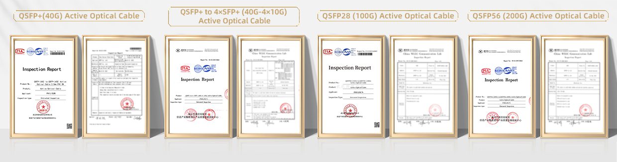
PRODUCT CERTIFICATION
COMPATIBLE BRANDS

CONFIGURATION INFORMATION
Related products
-
")
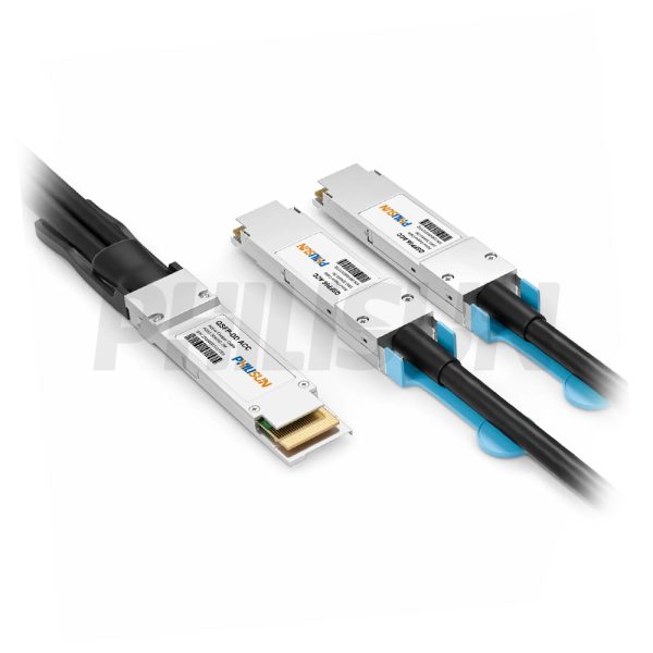
400G QSFP-DD to 4×100G QSFP56 Active Direct Attach Copper Twinax Cable (ACC)
Compliant with
QSFP-DD MSA, SFF-8636 standard
Switch to Switch
Switch to GPU -
")
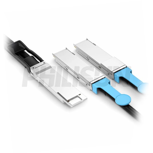
400G QSFP-DD to QSFP-DD Active Direct Attach Copper Twinax Cable (ACC)
Compliant with
QSFP-DD MSA, SFF-8636 standard
Switch to Switch
Switch to GPU