

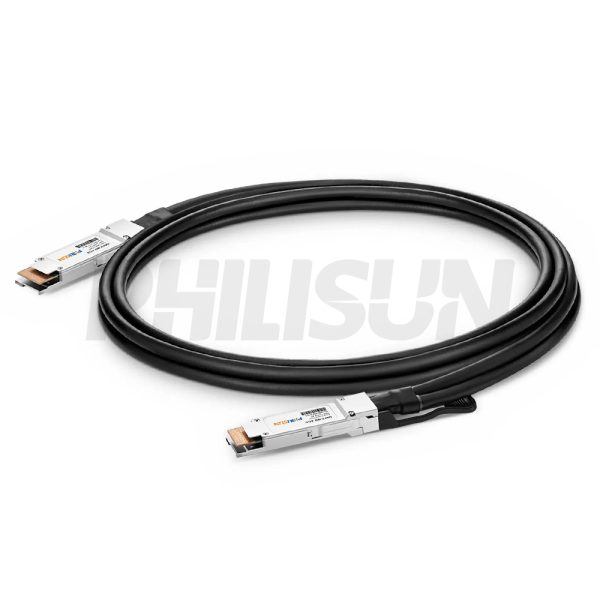
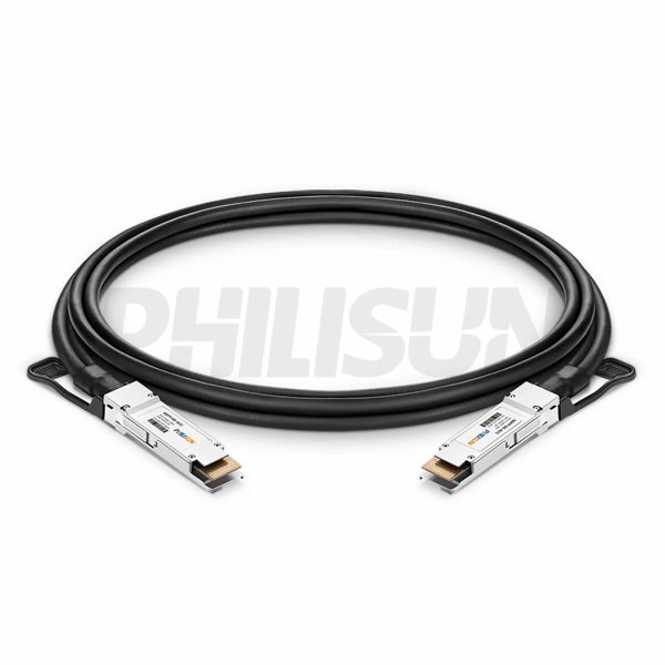
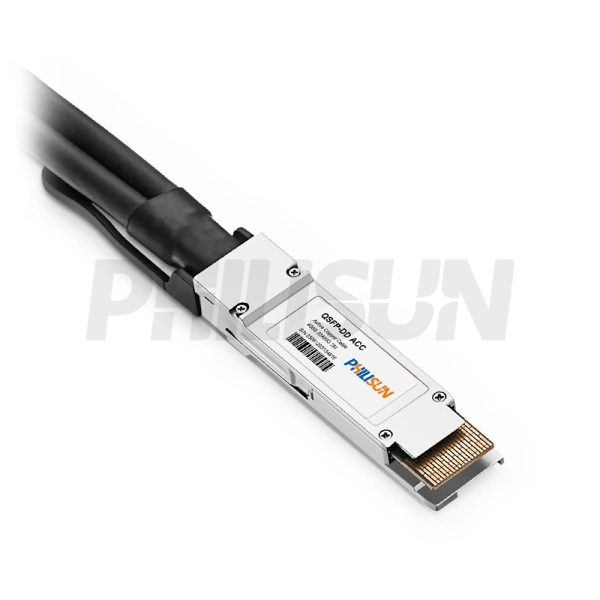
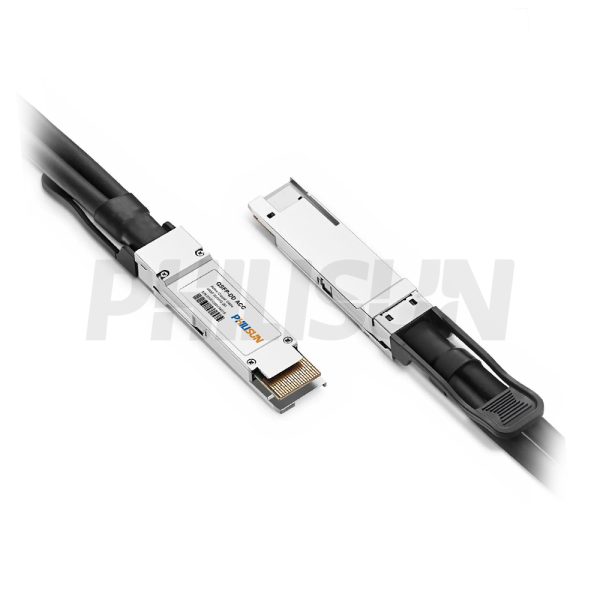
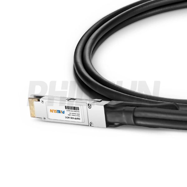
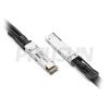
400G QSFP-DD to QSFP-DD Active Direct Attach Copper Twinax Cable (ACC)
Compliant with
QSFP-DD MSA, SFF-8636 standard
Switch to Switch
Switch to GPU
- High Quality
- Factory Outlet
- Satisfaction Guarantee
- Global Shipping
| SPECIFICATIONS | |||
|---|---|---|---|
| Cable End Connector A | QSFP-DD | Cable End Connector B | QSFP-DD |
| Jumper Type | Direct-Attach | Data Rate | 400G |
| Aggregate Bit Rate | 425Gbps | Lane Bit Rate | 53.125Gbps |
| Number of Channels | 8 | Single Channel Rate | 50G |
| Minimum Bend Radius | 5X Cable OD -Single, 10X Cable OD - Repeated | Factory Brand | PHILISUN |
| Attenuation | 26AWG:10dB/8.5m maximum 28AWG:10dB/7m maximum 30AWG:8.4dB/5.5m maximum | Bit Error Rate | ≤10-12 |
| Shield | Braid/Foil | Wire AWG | 26AWG/28AWG/30AWG |
| Cable Type | Active Twinax | Cable OD | 30AWG: 14.0mm 28AWG:16.0mm 26AWG:18.0mm |
| Cable Colour/Material | Black PVC(OFNR) | Cable Length Selection | 1-7meter |
| Protocols | QSFP112 MSA/SFF-8636 | Application Scenarios | 400Gigabit Ethernet (400GbE) |
| Supply Voltage | 3.3V | Power Dissipation | <2.5W |
| Operating Temperature | 0 to 70℃ (32 to 158℉) | Storage Temperature | -40 to 85℃ (-40 to 185℉) |
PRODUCT PRESENTATION
The PHILISUN 400G QSFP‑DD High‑Speed Active Twinax Cable delivers high‑quality connections without external power supply. Compliant with IEEE 802.3cd and SFF‑8636 MSA standards, it provides cost‑effective short‑reach interconnections for telecom central offices and data centers, supporting up to 400G LAN and SAN applications.
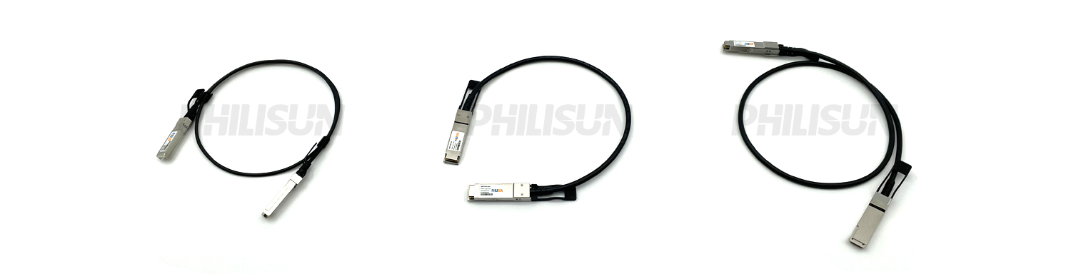
DAC SERIES PRODUCTS
PRODUCTION & TESTING EQUIPMENT

PERFORMANCE PARAMETER
| Absolute Maximum Ratings | |||||||||
| Parameter | Unit | Min. | Typ. | Max. | Notes | ||||
| Storage Temperature | ℃ | -45 | – | 80 | – | ||||
| Operating Relative Humidity | % | – | – | 85 | – | ||||
| Power Supply Not Damaged Voltage | V | -0.5 | – | 3.6 | – | ||||
| Recommended Operating Conditions | |||||||||
| Parameter | Unit | Min. | Typ. | Max. | Notes | ||||
| Operating Case Temperature | ℃ | 0 | – | 70 | – | ||||
| Power Supply Working Voltage | V | 3.135 | 3.3 | 3.65 | – | ||||
| Bit Rate | Gbps | – | 400 | – | – | ||||
| Characteristics | |||||||||
| All performance is defined over the recommended operating environment unless otherwise specified. | |||||||||
| Item | arameter | Reference | |||||||
| SDD21 | 8dB<X<17. 16dB @13.28 GHz | IEEE802.3cd, Clause 136.11.2 | |||||||
| SDD11/22 | ‘-16.5+2*sqrt(f)dB Max @0.05GHz- 4.1GHz -10.66+14*1og(f/5.5) dB Max@4.1GHz-19GHz |
– | |||||||
| SCD11/22 | -22+(20/25.78) *f dB Max@0.01GHz~12.89GHz -15+(6/25.78) *f dB Max@12.89GHz~19GHz |
IEEE802.3cd, Clause 136.11.4 | |||||||
| SCD21-SDD21 | ’-10dB Max @0.01GHz~12.89GHz -27+(29/22) *f dB Max @12.89GHz~15.7GHz -6.3dB Max. @15.7GHz~19GHz |
IEEE802.3cd, Clause 136.11.5 | |||||||
| SCC11/22 | -2dB Max. @0.2GHz~19GHz | IEEE802.3cd, Clause 136.11.6 | |||||||
| COM | 3 dB Min | – | |||||||
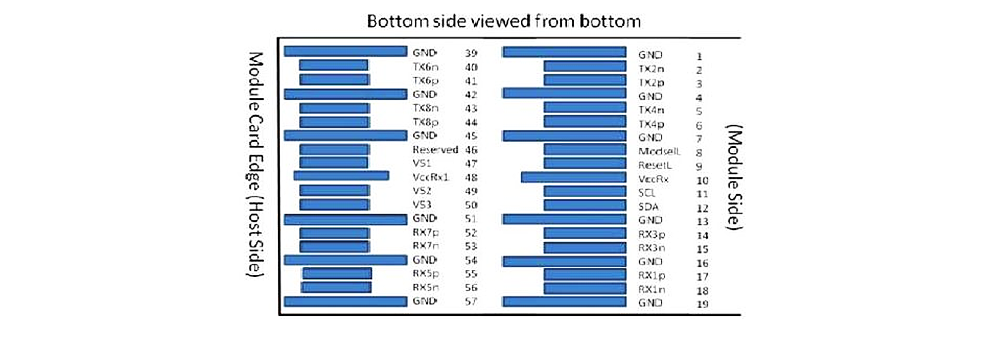
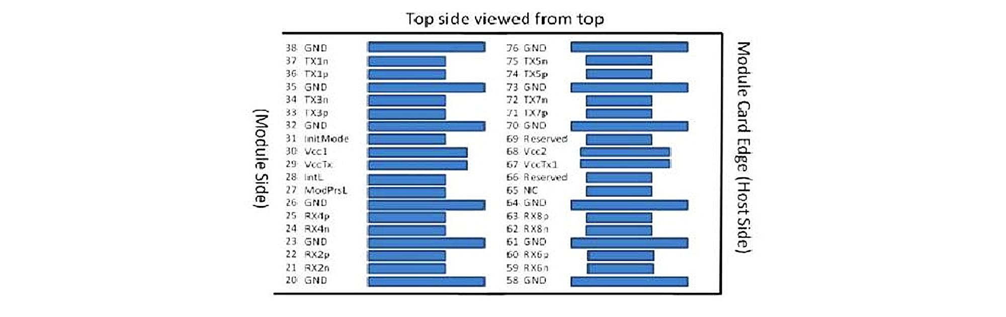
| Pin Function Definitions | |||||||||
| Pin No. | Symbol | Level / Logic | Definition | ||||||
| 1 | GND | – | Module Ground | ||||||
| 2 | Tx2n | CML-I | Transmitter Inverted Data Input | ||||||
| 3 | Tx2p | CML-I | Transmitter Non-Inverted Data Input | ||||||
| 4 | GND | – | Module Ground | ||||||
| 5 | Tx4n | CML-I | Transmitter Inverted Data Input | ||||||
| 6 | Tx4p | CML-I | Transmitter Non-Inverted Data Input | ||||||
| 7 | GND | – | Module Ground | ||||||
| 8 | ModSelL | LVTTL-I | – | ||||||
| 9 | ResetL | LVTTL-I | Module Reset | ||||||
| 10 | VccRx | – | +3.3V Power Supply for Receiver | ||||||
| 11 | SCL | LVTTL-I | 2-Wire Serial Interface Clock | ||||||
| 12 | SDA | LVTTL-I/O | 2-Wire Serial Interface Data Line | ||||||
| 13 | GND | – | Module Ground | ||||||
| 14 | Rx3p | CML-O | Receiver Non-Inverted Data Output | ||||||
| 15 | Rx3n | CML-O | Receiver Inverted Data Output | ||||||
| 16 | GND | – | Module Ground | ||||||
| 17 | Rx1p | CML-O | Receiver Non-Inverted Data Output | ||||||
| 18 | Rx1n | CML-O | Receiver Inverted Data Output | ||||||
| 19 | GND | – | Module Ground | ||||||
| 20 | GND | – | Module Ground | ||||||
| 21 | Rx2n | CML-O | Receiver Inverted Data Output | ||||||
| 22 | Rx2p | CML-O | Receiver Non-Inverted Data Output | ||||||
| 23 | GND | – | Module Ground | ||||||
| 24 | Rx4n | CML-O | Receiver Inverted Data Output | ||||||
| 25 | Rx4p | CML-O | Receiver Non-Inverted Data Output | ||||||
| 26 | GND | – | Module Ground | ||||||
| 27 | ModPrsL | LVTTL-O | Module Present | ||||||
| 28 | IntL/RxLOSL | LVTTL-O | Interrupt. Optionally configurable as RxLOSL via the management interface (SFF-8636). |
||||||
| 29 | VccTx | – | +3.3V Power Supply for Transmitter | ||||||
| 30 | Vcc1 | – | +3.3V Power Supply | ||||||
| 31 | LPMode/TxDis | LVTTL-I | Low Power Mode. Optionally configurable as TxDis via the management interface (SFF-8636). |
||||||
| 32 | GND | – | Module Ground | ||||||
| 33 | Tx3p | CML-I | Transmitter Non-Inverted Data Input | ||||||
| 34 | Tx3n | CML-I | Transmitter Inverted Data Input | ||||||
| 35 | GND | – | Module Ground | ||||||
| 36 | Tx1p | CML-I | Transmitter Non-Inverted Data Input | ||||||
| 37 | Tx1n | CML-I | Transmitter Inverted Data Input | ||||||
| 38 | GND | – | Module Ground | ||||||
| 39 | GND | – | Module Ground | ||||||
| 40 | Tx6n | CML-I | Transmitter Inverted Data Input | ||||||
| 41 | Tx6p | CML-I | Transmitter Non-Inverted Data Input | ||||||
| 42 | GND | – | Module Ground | ||||||
| 43 | Tx8n | CML-I | Transmitter Inverted Data Input | ||||||
| 44 | Tx8p | CML-I | Transmitter Non-Inverted Data Input | ||||||
| 45 | GND | – | Module Ground | ||||||
| 46 | Reserved | – | For future use | ||||||
| 47 | VSI | – | Module Vendor Specific 1 | ||||||
| 48 | VccRx1 | – | 3.3V Power Supply | ||||||
| 49 | VS2 | – | Module Vendor Specific 2 | ||||||
| 50 | VS3 | – | Module Vendor Specific 3 | ||||||
| 51 | GND | – | Module Ground | ||||||
| 52 | Rx7p | CML-O | Receiver Non-Inverted Data Output | ||||||
| 53 | Rx7n | CML-O | Receiver Inverted Data Output | ||||||
| 54 | GND | – | Module Ground | ||||||
| 55 | Rx5p | CML-O | Receiver Non-Inverted Data Output | ||||||
| 56 | Rx5n | CML-O | Receiver Inverted Data Output | ||||||
| 57 | GND | – | Module Ground | ||||||
| 58 | GND | – | Module Ground | ||||||
| 59 | Rx6n | CML-O | Receiver Inverted Data Output | ||||||
| 60 | Rx6p | CML-O | Receiver Non-Inverted Data Output | ||||||
| 61 | GND | – | Module Ground | ||||||
| 62 | Rx8n | CML-O | Receiver Inverted Data Output | ||||||
| 63 | Rx8p | CML-O | Receiver Non-Inverted Data Output | ||||||
| 64 | GND | – | Module Ground | ||||||
| 65 | NC | – | No Connect | ||||||
| 66 | Reserved | – | For future use | ||||||
| 67 | VccTx1 | – | 3.3V Power Supply | ||||||
| 68 | Vcc2 | – | 3.3V Power Supply | ||||||
| 69 | Reserved | – | For future use | ||||||
| 70 | GND | – | Module Ground | ||||||
| 71 | Tx7p | CML-I | Transmitter Non-Inverted Data Input | ||||||
| 72 | Tx7n | CML-I | Transmitter Inverted Data Input | ||||||
| 73 | GND | – | Module Ground | ||||||
| 74 | Tx5p | CML-I | Transmitter Non-Inverted Data Input | ||||||
| 75 | Tx5n | CML-I | Transmitter Inverted Data Input | ||||||
| 76 | GND | – | Module Ground | ||||||
Lectrical Pad Layout
For detail mechanical information, please refer to the related document of QSFP-DD MSA.
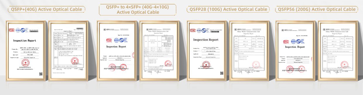
PRODUCT CERTIFICATION
COMPATIBLE BRANDS

CONFIGURATION INFORMATION
Related products
-
")
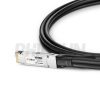
400G QSFP-DD to 2×200G QSFP56 Active Direct Attach Copper Twinax Cable (ACC)
Compliant with
QSFP-DD MSA, SFF-8636 standard
Switch to Switch
Switch to GPU -
")
400G QSFP-DD to 4×100G QSFP56 Active Direct Attach Copper Twinax Cable (ACC)
Compliant with
QSFP-DD MSA, SFF-8636 standard
Switch to Switch
Switch to GPU