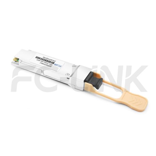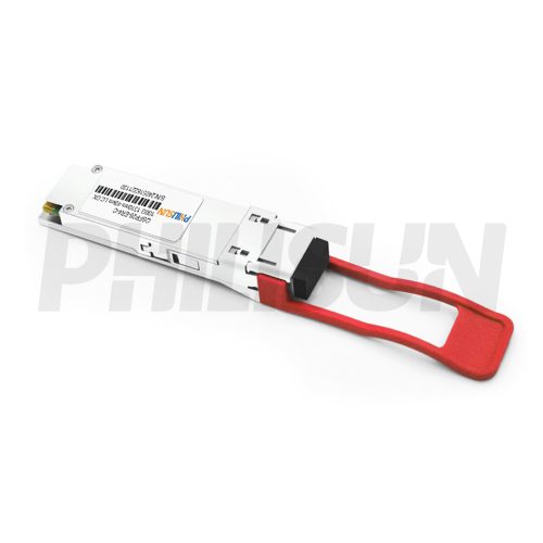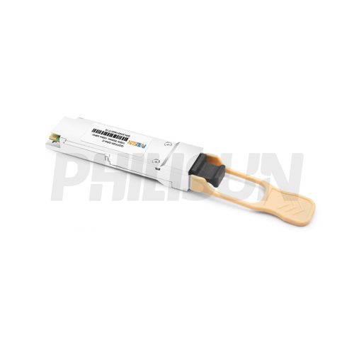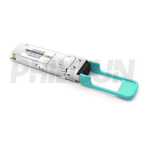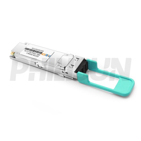
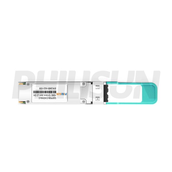
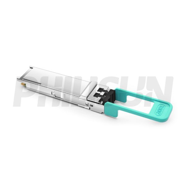
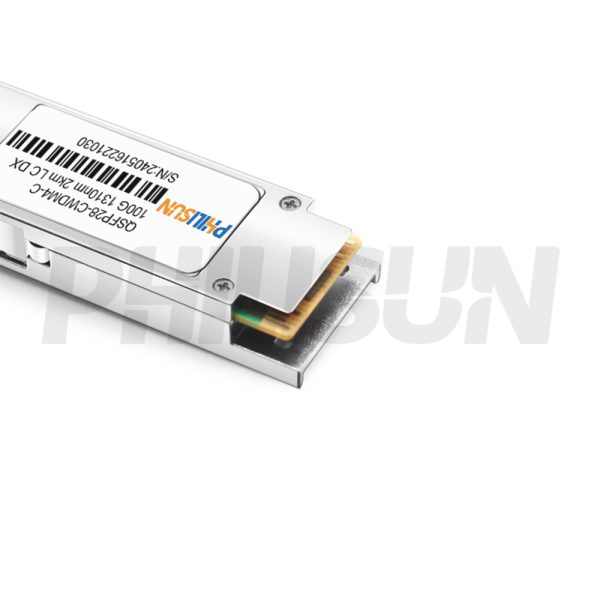
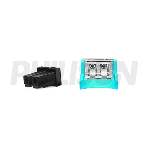
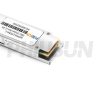
100G CWDM4 QSFP28 2km DOM Duplex LC SMF Optical Transceiver Module
100G CWDM4 QSFP28 optical transceiver with duplex LC, DOM and up to 2 km reach over single-mode fiber.
- High Quality
- Factory Outlet
- Satisfaction Guarantee
- Global Shipping
| SPECIFICATIONS | |||
|---|---|---|---|
| Product Model | QSFP28-103-CW4-2-LCD | Manufacturer brand | PHILISUN |
| Package Type | QSFP28 | Optical connector | LC DX |
| Max Data Rate | 100Gbps | Channel Data Rate | 25.78125Gbps |
| Effective transmission distance | 2km | ||
| Wavelength | 1310nm | Operating voltage | 3.3V |
| Fiber Type | SMF | Core Size | 9/125 |
| Transmitter Type | DFB | Receiver Type | IDP |
| TX Power | -6.5~2.5dBm | Receiver Sensitivity | -7.3dBm |
| Digital Optical Monitoring(DOM) | YES | Receiver Overload | 2.5dBm |
| Power Consumption | <3.5W | Protocols | SFF-8665: IEEE 802.3bm. IEEE 802.3ba. |
| Operating temperature(Commercial) | 0℃~+70℃ | Storage Temperature(Commercial) | -40℃~+85℃ |
PRODUCT PRESENTATION
The PHILISUN QSFP28 100G CWDM4 2km LC DX Transceiver is a compact and highly integrated 4x25G module, designed to deliver exceptional reach, bandwidth, density, and cost efficiency for high port-count 100G systems and client-side 100G interfaces. It adheres to the 100G 4WDM-10 MSA, based on CWDM4 MSA version 1.1, and ensures seamless interoperability with other CWDM4 transceivers over distances of up to 2km.
When to choose the 2 km CWDM4 module
This 2 km variant is intended for short-reach CWDM4 links over duplex LC single-mode fiber. It keeps the QSFP28 4 × 25G architecture while using the product-specific receiver limits shown below. Verify host FEC and total link loss against the 2 km table before deployment.
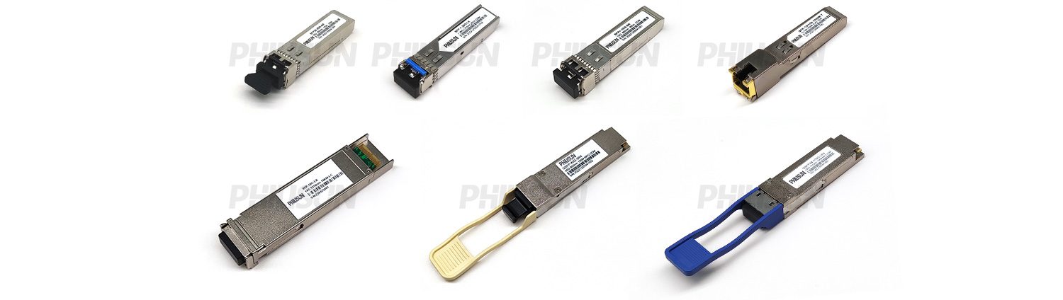
TRANSCEIVER SERIES PRODUCTS
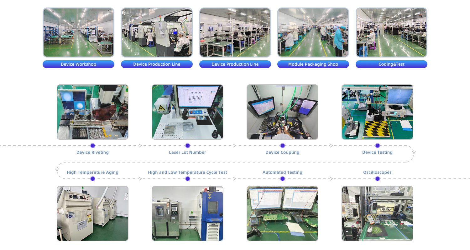
PRODUCTION & TESTING EQUIPMENT
PERFORMANCE PARAMETER
| Absolute Maximum Ratings | |||||||||
| Parameter | Symbol | Min. | Max. | Unit | |||||
| Power supply voltage | VCC | -0.5 | +3.6 | V | |||||
| Operating case temperature | TC | -40 | +85 | ℃ | |||||
| Relative humidity | RH | 5 | 85 | % | |||||
| These values represent the damage threshold of the module.Stress in excessof any of the individual absolute maximum ratings can cause immediate catastrophic damage tothe module even if all other parameters are within recommended operating conditions. | |||||||||
| Recommended Operating Environment | |||||||||
| Parameter | Symbol | Min | Typical | Max | Unit | ||||
| Power supply voltage | VCC | 3.15 | 3.30 | 3.45 | V | ||||
| Operating case temperature | Tca | 0 | – | 70 | ℃ | ||||
| Electrical Characteristics | |||||||||
| Parameter | Symbol | Min | Typical | Max | Unit | Ref | |||
| Transmitter | |||||||||
| Input differential impedance | Rin | – | 100 | – | Ω | 1 | |||
| Single-ended input voltage tolerance |
– | -0.3 | – | 4.0 | V | – | |||
| AC common mode input voltage tolerance |
– | 15 | – | – | mV | – | |||
| Differential input voltage | – | 50 | – | – | mV | – | |||
| Differential input voltage swing, perlane |
Vin | 190 | – | 1000 | mV | – | |||
| Receiver | |||||||||
| Output differential impedance | Rout | – | 100 | – | Ω | 1 | |||
| Differential output swing,perlane | Vout | 300 | – | 900 | mV | 2 | |||
| AC common mode output voltage tolerance |
– | – | – | 7.5 | mV | – | |||
| Single-ended output voltage | – | -0.3 | – | 4.0 | V | – | |||
| Notes: [1]AC coupled. [2]Into 100 ohm differentialter mination. |
|||||||||
| Transmitter Specifications-Optical | |||||||||
| Parameter | Symbol | Min | Typical | Max | Unit | – | |||
| Center wavelength | Ch0 | λ0 | 1264.5 | 1271 | 1277.5 | nm | – | ||
| Ch1 | λ1 | 1284.5 | 1291 | 1297.5 | nm | – | |||
| Ch2 | λ2 | 1304.5 | 1311 | 1317.5 | nm | – | |||
| Ch3 | λ3 | 1324.5 | 1331 | 1337.5 | nm | – | |||
| Bit rate per channel | DR | 25.78125±100p | Gbps | 1 | |||||
| Side mode suppression ratio | SMSR | 30 | – | – | dB | – | |||
| Average launch power each lane | – | -6.5 | – | 2.5 | dBm | 7 | |||
| Optical modulation amplitude(each lane) | OMA | -4.0 | 2.5 | dBm | – | ||||
| Transmit OMA per lane @TDP max | – | -2.0 | – | – |
 dBm
|
2 | |||
| l launch power in OMA minus TDP,each ane | OMA-TDP | -5.0 | – | – | dBm | – | |||
| Transmission&dispersion penalty, each lane | TDP | – | – | 3.0 | dB | 3 | |||
| Transmitter reflectance | – | – | – | -12 | dB | – | |||
| Extinction ratio | ER | 3.5 | – | – | dB | – | |||
| Transmitter eyemask definition{X1,X2,X3,Y1,Y2,Y3} | {0.31,0.4,0.45,0.34,0.38,0.4} CWDM4 MSA technical specifications rev 1.1 |
||||||||
| Total average launch power | Po | – | – | 8.5 | dBm | – | |||
| Average launch power of OFF transmitter,each lane | Poff | – | – | -30 | dBm | – | |||
| Optical return loss tolerance | ORL | – | – | 20 | dB | – | |||
| Receiver Specifications-Optical | |||||||||
| Parameter | Symbol | Min. | Typical | Max. | Unit | – | |||
| Center wavelength | Ch0 | λ0 | 1264.5 | 1271 | 1277.5 | nm | – | ||
| Ch1 | λ1 | 1284.5 | 1291 | 1297.5 | nm | – | |||
| Ch2 | λ2 | 1304.5 | 1311 | 1317.5 | nm | – | |||
| Ch3 | λ3 | 1324.5 | 1331 | 1337.5 | nm | – | |||
| BitRate per channel | DR | 25.78125±100ppm | Gbps | 4 | |||||
| Unstressed sensitivity(OMA) | OMAin | – | – | -10 | dBm | 5 | |||
| Receiver overload | PMAX | 2.5 | – | – | – | – | |||
| Stressed sensitivity(OMA) | OMAin,str | – | – | -7.3 | dBm | 6 | |||
| Optical return loss | ORL | – | – | -26 | dB | – | |||
| Vertical eye closure penalty,each lane | VECP | – | – | 1.9 | dB | – | |||
| Stressed eye J2 jitter,each lane | J2 | – | – | 0.3 | UI | – | |||
| Stressed eye J9 jitter,each lane | J9 | – | – | 0.5 | UI | – | |||
| Stressed eye J4 jitter,each lane | J4 | – | – | 0.48 | UI | – | |||
| SRS eye mask definition{X1,X2,X3,Y1, Y2,Y3} | {0.39,0.5,0.5,0.39,0.39,0.4} CWDM4 MSA Technical Specifications Rev 1.1 |
– | |||||||
| Damage threshold,eachlane | – | 3.5 | – | – | dB | – | |||
| Notes: [1]Transmitter consists of 4lasersoperating at25.78Gb/s each. [2]At maximum TDP. [3]TDP value does not include MPI penalty. [4]Receiver consists of4 photodetectors operating at 25.78Gb/s each. [5]Sensitivity is specified at 5×10⁻⁵ BER. [6]Measured with CWDM4 MSA2 conformance test signal at TP3 for 5×10⁻⁵BER. [7]Power value and power accuracy are with allchannels on. |
|||||||||
| General Specifications | |||||||||
| Parameter | Symbol | Min. | Typical | Max. | Unit | Ref. | |||
| Bit rate(all wavelengths combined) | BR | – | – | 103.1 | Gb/s | – | |||
| BitError ratio @25.78Gb/s | BER | – | – | 5×10-⁵ | – | 1 | |||
| Maximum supported distances | |||||||||
| Fiber type | – | – | – | – | – | – | |||
| SMF per G.652 | LossBdgt | – | – | 5 | dB | 2 | |||
| Notes: [1]Tested with a 231-1PRBS. [2]This 5dB loss budget includes2.5dB optical coding gain from FEC on the host [RS-FEC(528,514)per Clause 91].The maximum informative link lengthis 2km.The option to bypass RS-FEC is not supported.Loss budget may include upto 1dB MPIloss penalty with worse caseTransmitter and worst case connector MPI. |
|||||||||
QSFP28 TRANSCEIVER ELECTRICAL PAD LAYOUT
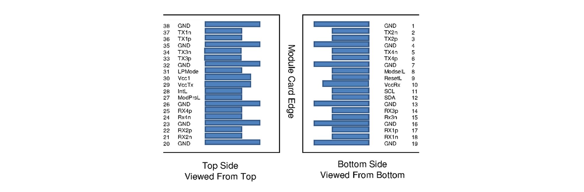
PIN DEFINITION
| Pin Definition | |||||||||
| Pin | Symbol | Name/Description | |||||||
| 1 | GND | Ground | |||||||
| 2 | Tx2n | Transmitter inverted data input | |||||||
| 3 | Tx2p | Transmitter non-inverted data input | |||||||
| 4 | GND | Ground | |||||||
| 5 | Tx4n | Transmitter inverted data input | |||||||
| 6 | Tx4p | Transmitter non-inverted data input | |||||||
| 7 | GND | Ground | |||||||
| 8 | ModSelL | Module select | |||||||
| 9 | ResetL | Module reset | |||||||
| 10 | VCCRx | +3.3V power supply receiver | |||||||
| 11 | SCL | 2-wire serial interface clock | |||||||
| 12 | SDA | 2-wire serial interface data | |||||||
| 13 | GND | Ground | |||||||
| 14 | Rx3p | Receiver non-inverted data output | |||||||
| 15 | Rx3n | Receiver inverted data output | |||||||
| 16 | GND | Ground | |||||||
| 17 | Rxlp | Receiver non-inverted data output | |||||||
| 18 | Rx1n | Receiver inverted data output | |||||||
| 19 | GND | Ground | |||||||
| 20 | GND | Ground | |||||||
| 21 | Rx2n | Receiver inverted data output | |||||||
| 22 | Rx2p | Receiver non-inverted data output | |||||||
| 23 | GND | Ground | |||||||
| 24 | Rx4n | Receiver inverted data output | |||||||
| 25 | Rx4p | Receiver non-inverted data output | |||||||
| 26 | GND | Ground | |||||||
| 27 | ModPrsL | Module present | |||||||
| 28 | IntL | Interrupt | |||||||
| 29 | VCCTx | +3.3V power supply transmitter | |||||||
| 30 | VCC1 | +3.3V power supply | |||||||
| 31 | LPMode | Low power mode | |||||||
| 32 | GND | Ground | |||||||
| 33 | Tx3p | Transmitter non-inverted data input | |||||||
| 34 | Tx3n | Transmitter inverted data input | |||||||
| 35 | GND | Ground | |||||||
| 36 | Txlp | Transmitter non-inverted data input | |||||||
| 37 | Tx1n | Transmitter inverted data input | |||||||
| 38 | GND | Ground | |||||||
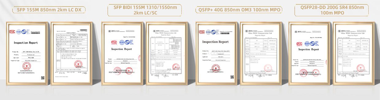
PRODUCT CERTIFICATION
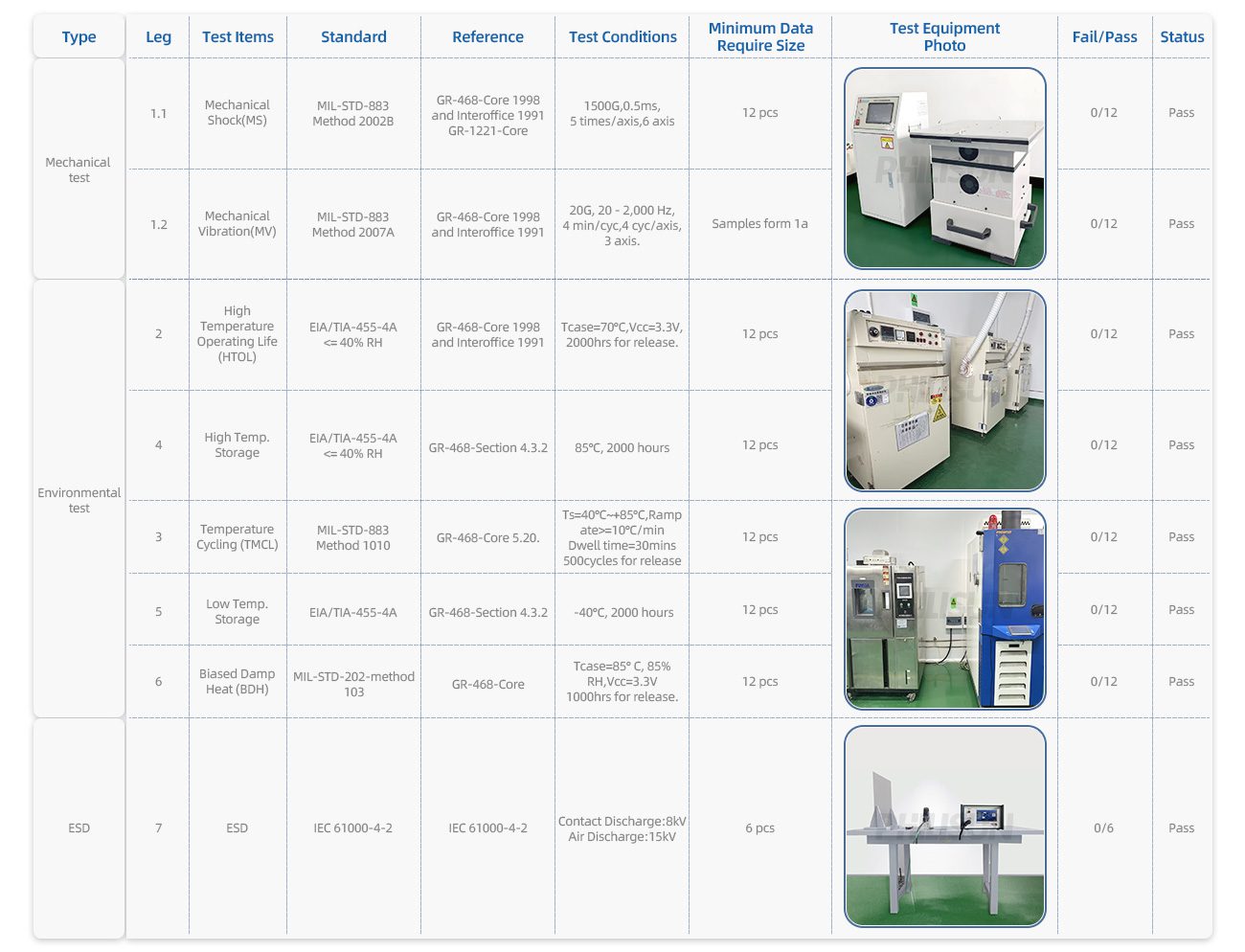
QUALITY ADVANTAGE
COMPATIBLE BRANDS

CONFIGURATION INFORMATION