

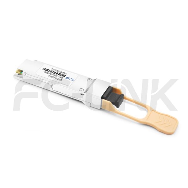
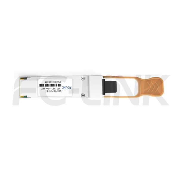
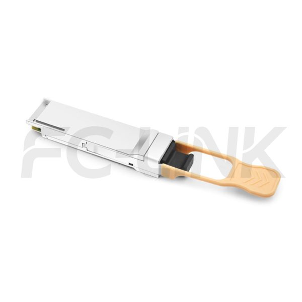
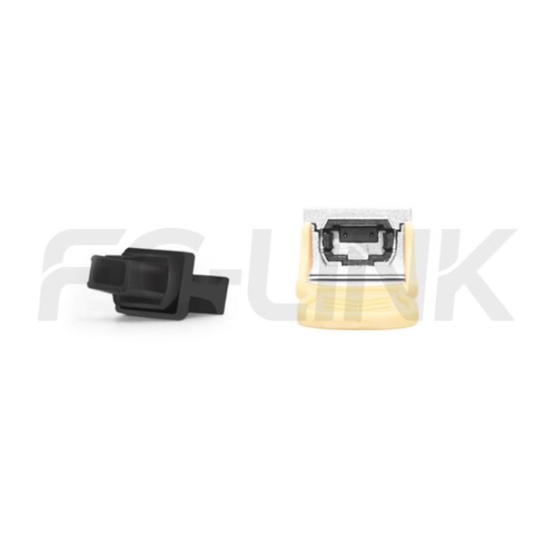
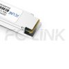
100G QSFP28 PSM4 2km DOM MPO8/12 SMF Optical Transceiver Module
QSFP28-103-PS4-2-MPO8/12
- High Quality
- Factory Outlet
- Satisfaction Guarantee
- Global Shipping
| SPECIFICATIONS | |||
|---|---|---|---|
| Product Model | QSFP28-103-PS4-2-MPO8/12 | Manufacturer brand | PHILISUN |
| Package Type | QSFP28 | Optical connector | MPO 8C/12C |
| Max Data Rate | 100Gbps | Channel Data Rate | 26Gbps |
| Effective transmission distance | 2km | ||
| Wavelength | 1310nm | Operating voltage | 3.3V |
| Fiber Type | SMF | Core Size | 9/125 |
| Transmitter Type | DFB | Receiver Type | PIN |
| TX Power | -9.4~2.0dBm | Receiver Sensitivity | -11.35dBm |
| Digital Optical Monitoring(DOM) | YES | Receiver Overload | 2.5dBm |
| Power Consumption | <3.5W | Protocols | 100G Ethernet Proprietary High Speed Interconnections Data center |
| Operating temperature(Commercial) | 0℃~+70℃ | Storage Temperature(Commercial) | -40℃~+85℃ |
PRODUCT PRESENTATION
The PHILISUN QSFP28 100G PSM4 2km MPO 8/12 is a high-performance, four-channel pluggable parallel fiber-optic transceiver designed for 100G Ethernet applications. This full-duplex module features four independent transmit and receive channels, each supporting 26Gbps, delivering a total aggregate data rate of 104Gbps over distances of up to 2km on single-mode fiber.Equipped with a 1310nm DFB laser array, the transceiver connects via an MPO/MTP optical fiber ribbon cable. As a parallel transceiver, the QSFP28 PSM4 enhances port density and reduces total system costs, making it an efficient solution for high-speed networking environments.
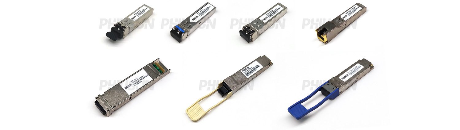
TRANSCEIVER SERIES PRODUCTS
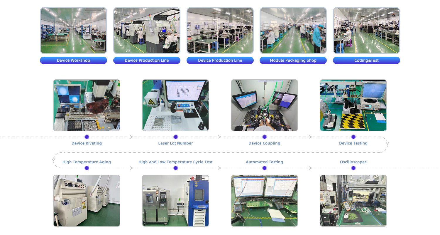
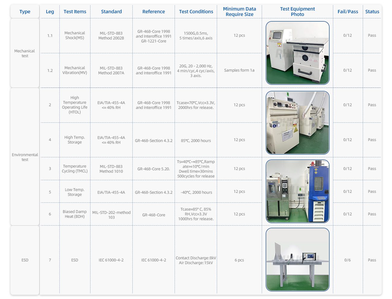
PRODUCTION & TESTING EQUIPMENT
PERFORMANCE PARAMETER
| Absolute Maximum Ratings | |||||||||
| Parameter | Symbol | Min. | Max. | Unit | |||||
| Power supply voltage | VCC | -0.3 | +3.6 | V | |||||
| Storage temperature | TC | -40 | +85 | ℃ | |||||
| Relative humidity | RH | 0 | 85 | % | |||||
| Recommended Operating Environment | |||||||||
| Parameter | Symbol | Min | Typical | Max | Unit | ||||
| Power supply voltage | VCC | 3.135 | 3.30 | 3.465 | V | ||||
| Operating case temperature | Tca | 0 | – | 70 | ℃ | ||||
| Electrical Characteristics | |||||||||
| Parameter | Symbol | Min | Typical | Max | Unit | Ref | |||
| Transmitter | |||||||||
| Input differential impedance | Rin | – | 100 | – | Ω | 1 | |||
| Differential input voltage amplitude | △Vin | 300 | – | 1100 | mVp-p | – | |||
| Input logic level high | VIH | 2.0 | – | VCC | V | – | |||
| Input logic level low | VIL | 0 | – | 0.8 | V | – | |||
| Receiver | |||||||||
| Output differential impedance | Rout | – | 100 | – | Ω | 1 | |||
| Differential output swing,per lane | Vout | 300 | – | 800 | mVp-p | 2 | |||
| Output logic level high | VOH | VCC-0.5 | – | VCC | V | – | |||
| Output logic level low | VOL | 0 | – | 0.4 | V | – | |||
| Notes: [1]AC coupled. [2]Into 100 ohm differential termination. |
|||||||||
| Transmitter Specifications-Optical | |||||||||
| Parameter | Symbol | Min | Typical | Max | Unit | – | |||
| Center wavelength | λC | 1295 | – | 1325 | nm | 1 | |||
| RMS spectral width | λrms | – | – | 3.5 | nm | 1 | |||
| Average launch power, each lane | PAVG | -9.4 | – | 2.0 | dBm | – | |||
| Optical modulation amplitude(OMA) | POMA | -4 | – | 2.2 | dBm | 1 | |||
| Difference in launch power between any two lanes | Ptx,diff | – | – | 5.0 | dB | – | |||
| Transmitter and dispersion penalty(TDP), each lane(max) |
TDP | – | – | 2.9 | dBm | 1 | |||
| Rise/Fall time | Tr/Tf | – | – | 30 | ps | – | |||
| Extinction ratio | ER | 3.5 | – | – | dB | – | |||
| Relative intensity noise | Rin | – | – | -128 | dB/Hz | – | |||
| Optical return loss tolerance | TOL | – | – | 20 | dB | – | |||
| Transmitter reflectance | RT | – | – | -12 | dB | – | |||
| Transmitter eye mask margin | EMM | 10 | – | – | % | 2 | |||
| Transmitter eye mask definition {X1,X2, X3,Y1,Y2,Y3} |
– | [0.31,0.4,0.45,0.34,0.38,0.4} | – | – | |||||
| Average launch power OFF transmitter, each lane |
Poff | -30 | dBm | – | |||||
| Receiver Specifications-Optical | |||||||||
| Parameter | Symbol | Min. | Typical | Max. | Unit | – | |||
| Center wavelength | λC | 1295 | – | 1325 | nm | – | |||
| Damage threshold | THd | +3 | – | – | dBm | – | |||
| Overload,each lane | OVL | +2.5 | – | – | dBm | – | |||
| Receiver sensitivity in OMA,each Lane | SEN | – | – | -11.35 | dBm | – | |||
| Difference in receive power between any two lanes(OMA) | Prx,diff | – | – | 5 | dB | – | |||
| Signal loss assert threshold | LOSA | -30 | – | – | dBm | – | |||
| Signal loss de-assert threshold | LOSD | – | – | -12 | dBm | – | |||
| LOS hysteresis | LOSH | 0.5 | – | – | dB | – | |||
| Optical return Loss | ORL | – | – | -12 | dBm | – | |||
| Notes: [1]Transmitter wavelength,RMS spectral width and power need to meet the OMAm inus TDP specs to guarantee link performance. [2]The eyediagram is tested with 1000 waveform. |
|||||||||
QSFP28 TRANSCEIVER ELECTRICAL PAD LAYOUT
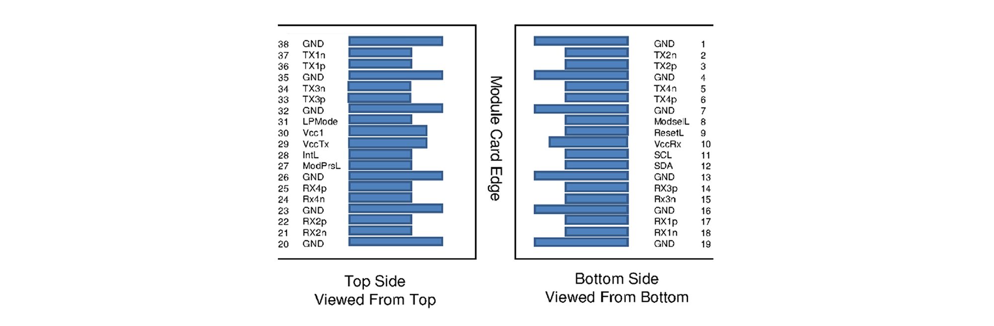
PIN DEFINITION
| Pin Definition | |||||||||
| Pin | Symbol | Name/Description | |||||||
| 1 | GND | Ground | |||||||
| 2 | Tx2n | Transmitter inverted data input | |||||||
| 3 | Tx2p | Transmitter non-inverted data input | |||||||
| 4 | GND | Ground | |||||||
| 5 | Tx4n | Transmitter inverted data input | |||||||
| 6 | Tx4p | Transmitter non-inverted data input | |||||||
| 7 | GND | Ground | |||||||
| 8 | ModSelL | Module select | |||||||
| 9 | ResetL | Module reset | |||||||
| 10 | VCCRx | +3.3V power supply receiver | |||||||
| 11 | SCL | 2-wire serial interface clock | |||||||
| 12 | SDA | 2-wire serial interface data | |||||||
| 13 | GND | Ground | |||||||
| 14 | Rx3p | Receiver non-inverted data output | |||||||
| 15 | Rx3n | Receiver inverted data output | |||||||
| 16 | GND | Ground | |||||||
| 17 | Rxlp | Receiver non-inverted data output | |||||||
| 18 | Rx1n | Receiver inverted data output | |||||||
| 19 | GND | Ground | |||||||
| 20 | GND | Ground | |||||||
| 21 | Rx2n | Receiver inverted data output | |||||||
| 22 | Rx2p | Receiver non-inverted data output | |||||||
| 23 | GND | Ground | |||||||
| 24 | Rx4n | Receiver inverted data output | |||||||
| 25 | Rx4p | Receiver non-inverted data output | |||||||
| 26 | GND | Ground | |||||||
| 27 | ModPrsL | Module present | |||||||
| 28 | IntL | Interrupt | |||||||
| 29 | VCC Tx | +3.3V power supply transmitter | |||||||
| 30 | VCC1 | +3.3V power supply | |||||||
| 31 | LPMode | Low power mode | |||||||
| 32 | GND | Ground | |||||||
| 33 | Tx3p | Transmitter non-inverted data input | |||||||
| 34 | Tx3n | Transmitter inverted data input | |||||||
| 35 | GND | Ground | |||||||
| 36 | Txlp | Transmitter non-inverted data input | |||||||
| 37 | Tx1n | Transmitter inverted data input | |||||||
| 38 | GND | Ground | |||||||
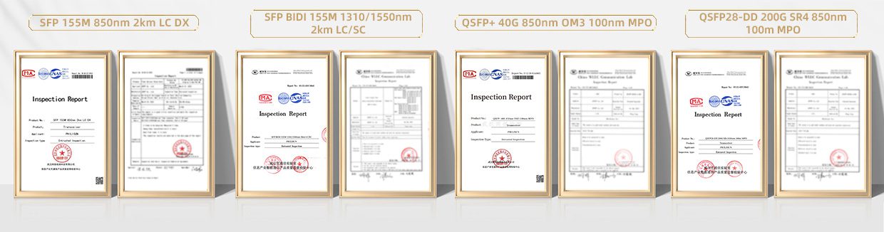
PRODUCT CERTIFICATION
QUALITY ADVANTAGE
COMPATIBLE BRANDS

CONFIGURATION INFORMATION
Related products
-
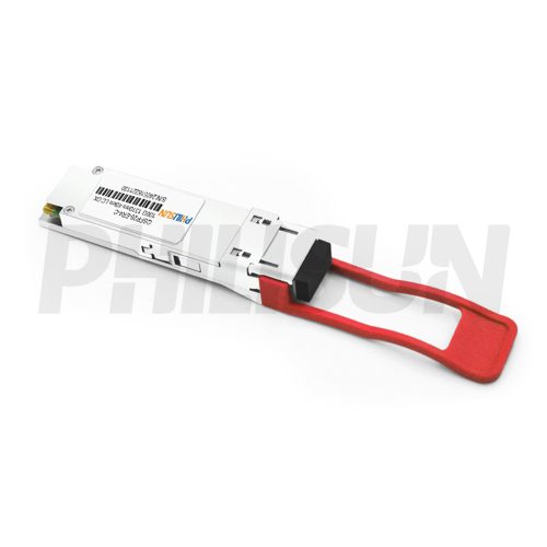
100G QSFP28 40km DOM Duplex LC SMF Optical Transceiver Module
QSFP28-103/112-LW-40(ER4)-LCD
-
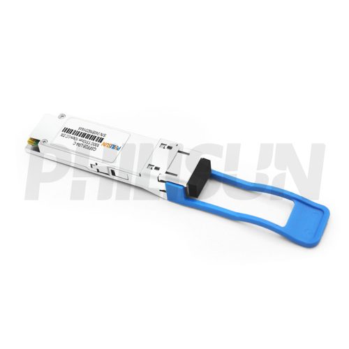
100G QSFP28 10km DOM Duplex LC SMF Optical Transceiver Module
QSFP28-103-LW-10(LR4)-LCD
-
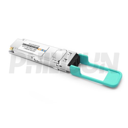
100G CWDM4 QSFP28 2km DOM Duplex LC SMF Optical Transceiver Module
100G CWDM4 QSFP28 optical transceiver with duplex LC, DOM and up to 2 km reach over single-mode fiber.
-
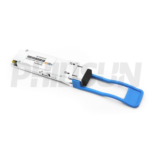
100G QSFP28 10km Breakout DOM Duplex LC SMF Optical Transceiver Module
QSFP28-103-LW-10(LR4)-LCD-OUT4