

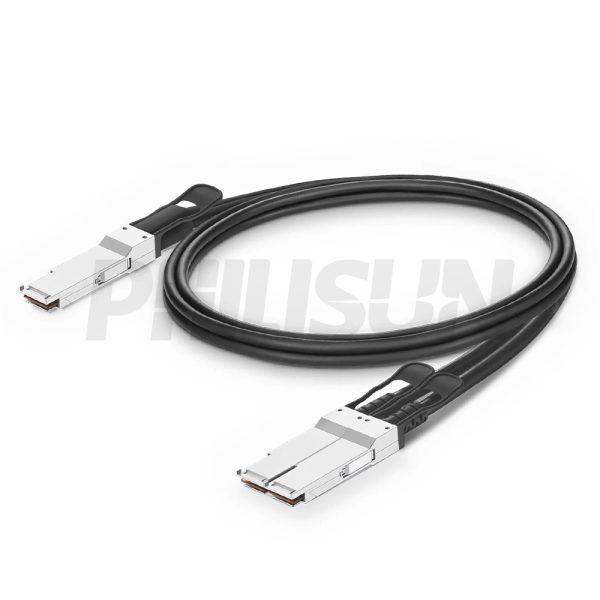
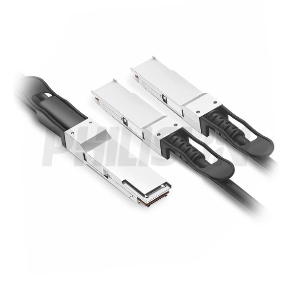
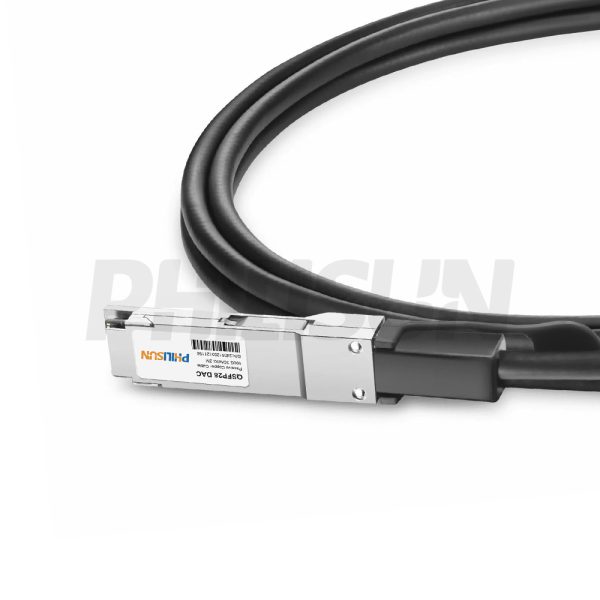
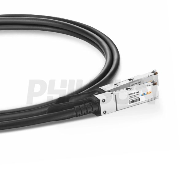
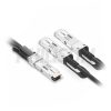
100G QSFP28 to 2×50G QSFP28 Passive Direct Attach Copper Twinax Cable (DAC)
Compliant with IEEE 802.3、SFF-8665、SFF-8636、QSFP28 MSA standard
Switch to Switch
Switch to GPU
- High Quality
- Factory Outlet
- Satisfaction Guarantee
- Global Shipping
| SPECIFICATIONS | |||
|---|---|---|---|
| Cable End Connector A | QSFP28 | Cable End Connector B | 2×QSFP28 |
| Jumper Type | Direct-Attach Breakout | Data Rate | 100G |
| Aggregate Bit Rate | 103.125Gbps | Lane Bit Rate | 25.78125Gbps |
| Number of Channels | 4 | Single Channel Rate | 25G |
| Minimum Bend Radius | 5X Cable OD -Single, 10X Cable OD - Repeated | Factory Brand | PHILISUN |
| Attenuation | 26AWG:10dB/8.5m maximum 30AWG:8.4dB/5.5m maximum | Bit Error Rate | ≤10-12 |
| Shield | Braid/Foil | Wire AWG | 26AWG/30AWG |
| Cable Type | Passive Twinax | Cable OD | 30AWG: 5.9mm 26AWG: 6.3mm |
| Cable Colour/Material | Black PVC(OFNR) | Cable Length Selection | 0.5-5 meter |
| Protocols | IEEE 802.3bj/SFF-8665/SFF-8679/ SFF-8636/ SFF-8661/QSFP28 MSA | Application Scenarios | 100 to 2x50Gigabit Ethernet (100GbE) 128G Fibre Channel |
| Supply Voltage | 3.3V | Power Dissipation | <0.5W |
| Operating Temperature | 0 to 70℃ (32 to 158℉) | Storage Temperature | -40 to 85℃ (-40 to 185℉) |
PRODUCT PRESENTATION
The PHILISUN 100G QSFP28 to 2x50G QSFP28 Passive Direct Attach Copper Twinax Cable (DAC) is a flexible Breakout Cable solution, converting a single 100G port into two independent 50G QSFP28 links. This Passive Copper DAC Cable is crucial for maximizing port density in Data Center racks. It delivers Low Latency and is highly Cost-Effective, compliant with the IEEE 802.3, SFF-8665, SFF-8636, and QSFP28 MSA Standard. It is ideal for scalable Switch to Switch aggregation and connections from Switch to GPU to lower-speed servers.
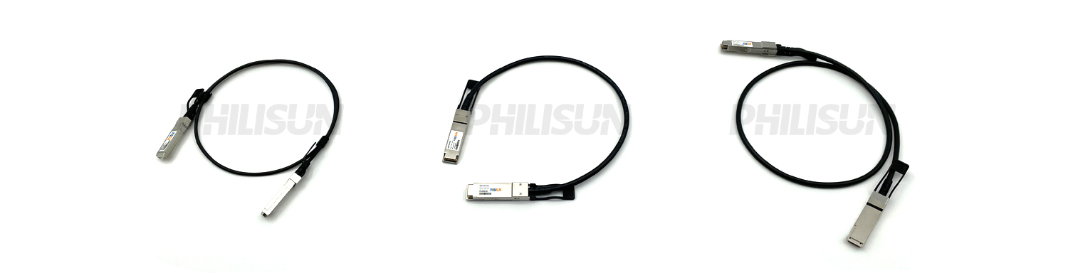
DAC SERIES PRODUCTS
PRODUCTION & TESTING EQUIPMENT

PERFORMANCE PARAMETER
| General Product Characteristics | |||||||||
| Compliance Standard | IEEE 802.3bj/SFF-8665/SFF-8679/ SFF-8636/ SFF-8661 | ||||||||
| Number of Lanes | 4 Tx & 4 Rx | ||||||||
| Channel Data Rate | 25.78125 Gbps/channe | ||||||||
| Operating Case Temperature | 0 to + 70°C | ||||||||
| Storage Temperature | -40 to + 85°C | ||||||||
| Supply Voltage | 3.3V nominal | ||||||||
| Electrical Interface | 38-pin edge connector | ||||||||
| Management Interface | Serial, 12C | ||||||||
Pin Function Definition
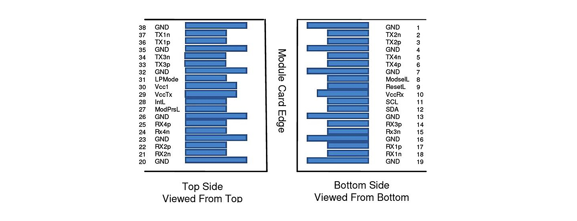
| PIN | Logic | Symbol | Description | Plug Sequence | Note | ||||
| 1 | – | GND | Ground | 1 | 1 | ||||
| 2 | CML-I | Tx2n | Transmitter Inverted Data Input | 3 | – | ||||
| 3 | CML-I | Tx2p | Transmitter Non-inverted Data Input | 3 | – | ||||
| 4 | – | GND | Ground | 1 | 1 | ||||
| 5 | CML-I | Tx4n | Transmitter Inverted Data Input | 3 | – | ||||
| 6 | CML-I | Tx4p | Transmitter Non-inverted Data Input | 3 | – | ||||
| 7 | – | GND | Ground | 1 | 1 | ||||
| 8 | LVTTL-I | ModSeIL | Module Select | 3 | – | ||||
| 9 | LVTTL-I | ResetL | Module Reset | 3 | – | ||||
| 10 | – | VccRx | +3.3V Power Supply Receiver | 2 | – | ||||
| 11 | LVCMOS-I/O | SCL | 2-Wire Serial Interface Clock | 3 | 2 | ||||
| 12 | LVCMOS-I/O | SDA | 2-Wire Serial Interface Data | 3 | 2 | ||||
| 13 | – | GND | Ground | 1 | 1 | ||||
| 14 | CML-O | Rx3p | Receiver Non-Inverted Data Output | 3 | – | ||||
| 15 | CML-O | Rx3n | Receiver Inverted Data Output | 3 | – | ||||
| 16 | – | GND | Ground | 1 | 1 | ||||
| 17 | CML-O | Rx1p | Receiver Non-Inverted Data Output | 3 | – | ||||
| 18 | CML-O | Rx1n | Receiver Inverted Data Output | 3 | – | ||||
| 19 | – | GND | Ground | 1 | 1 | ||||
| 20 | – | GND | Ground | 1 | 1 | ||||
| 21 | CML-O | Rx2n | Receiver Inverted Data Output | 3 | – | ||||
| 22 | CML-O | Rx2p | Receiver Non-Inverted Data Output | 3 | – | ||||
| 23 | – | GND | Ground | 1 | 1 | ||||
| 24 | CML-O | Rx4n | Receiver Inverted Data Output | 3 | – | ||||
| 25 | CML-O | Rx4p | Receiver Non-Inverted Data Output | 3 | – | ||||
| 26 | – | GND | Ground | 1 | 1 | ||||
| 27 | LVTTL-O | ModPrsL | Module Present | 3 | 2 | ||||
| 28 | LVTTL-O | IntL | Interrupt | 3 | 2 | ||||
| 29 | – | VccTx | +3.3V Power Supply Transmitter | 2 | – | ||||
| 30 | – | Vcc1 | +3.3V Power Supply | 2 | – | ||||
| 31 | LVTTL-1 | LPMode | Low Power Mode | 3 | – | ||||
| 32 | – | GND | Ground | 1 | 1 | ||||
| 33 | CML-I | Tx3p | Transmitter Non-Inverted Data Input | 3 | – | ||||
| 34 | CML-I | Tx3n | Transmitter Inverted Data Input | 3 | – | ||||
| 35 | – | GND | Ground | 1 | 1 | ||||
| 36 | CML-I | Tx1p | Transmitter Non-Inverted Data Input | 3 | – | ||||
| 37 | CML-I | Tx1n | Transmitter Inverted Data Input | 3 | – | ||||
| 38 | – | GND | Ground | 1 | 1 | ||||
| Notes: 1,GND is the symbol for signal and supply (power) common for QSFP modules. All are common within the QSFP module and all modulevoltages are referenced to this potential unless otherwise noted. Connect these directly to the host board signal common ground plane. 2,VccRx, Vcc1 and VccTx are the receiver and transmitter power suppliers and shall be applied concurrently. Recommended host board power supply filtering is shown below. Vcc Rx, Vcc1 and Vcc Tx may be internally connected within the QSFP transceiver module in any combination. The connector pins are each rated for a maximum current of 1000mA. |
|||||||||
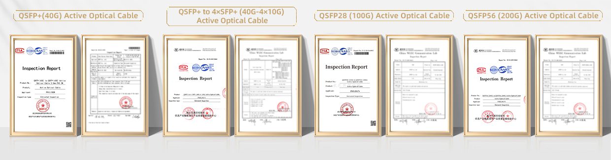
PRODUCT CERTIFICATION
COMPATIBLE BRANDS

CONFIGURATION INFORMATION
Related products
-

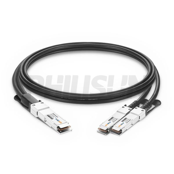
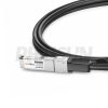
100G QSFP28 to QSFP28 Passive Direct Attach Copper Twinax Cable (DAC)
Compliant with IEEE 802.3、SFF-8662、QSFP28 MSA standard
Switch to Switch
Switch to GPU -

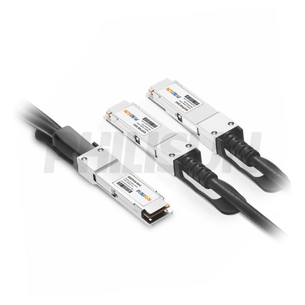
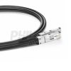
100G QSFP28 to 4×25G SFP28 Passive Direct Attach Copper Twinax Cable (DAC)
Compliant with IEEE 802.3、SFF-8665、SFF-8636、QSFP28 MSA standard
Switch to Switch
Switch to GPU