

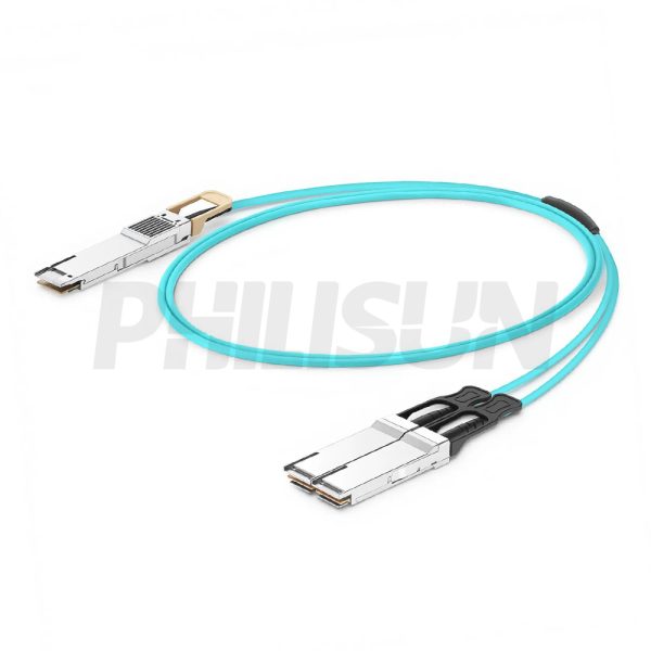
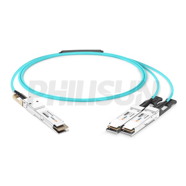
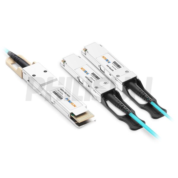
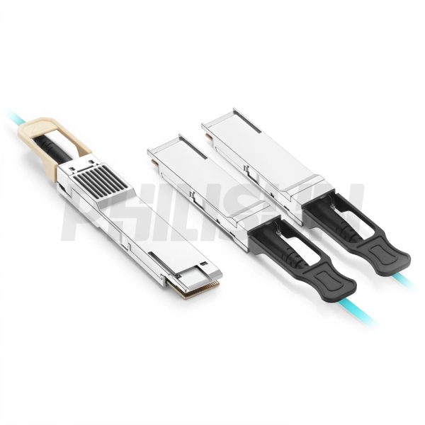

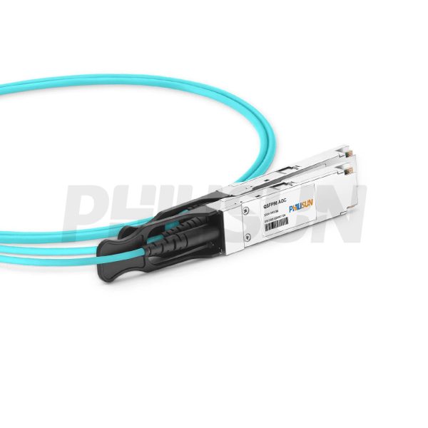
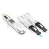
400G QSFP-DD to 2×200G QSFP56 Active Optical Cable(AOC)
Compliant with IEEE 802.3、QSFP-DD MSA、SFF-8024、SFF-8679、SFF-8665、OIF-CEI-04.0、CMIS 4.0 standard
Switch to Switch
Switch to GPU
- High Quality
- Factory Outlet
- Satisfaction Guarantee
- Global Shipping
| SPECIFICATIONS | |||
|---|---|---|---|
| Cable End Connector A | QSFP-DD | Cable End Connector B | 2×QSFP56 |
| Jumper Type | Active Optical Breakout Cable | Data Rate | 400G |
| Aggregate Bit Rate | 425Gbps | Lane Bit Rate | 53.125Gbps |
| Number of Channels | 8 | Single Channel Rate | 50G |
| Array Transmitter | VSCEL | Array Receiver | PIN |
| Minimum Bend Radius | 30mm | Factory Brand | PHILISUN |
| Center(Operating) Wavelength | 850nm | Bit Error Rate | 2.4E-4 |
| Fiber Type | OM3 MMF MAX 70m/OM4 MMF MAX 100m | Cable Colour | Aqua |
| Cable Material | LSZH/OFNP | Cable Length Selection | 1-100meter |
| Safety Certification | TUV/UL/FDA | Application Scenarios | 400 Gigabit Ethernet (400GbE) |
| Protocols | QSFP-DD MSA/QSFP-DD-CMIS-Rev4.0/SFF-8024 Rev.4.6/SFF-8679 Rev1.8/SFF-8665 Rev1.9/IEEE 802.3cd/IEEE 802.3bs Annex120E | DDMI(Commercial) | YES |
| Supply Voltage | 3.3V | Power Dissipation | QSFP-DD:<11.0W QSFP56:<5.0W |
| Operating Temperature | 0 to 70℃ (32 to 158℉) | Storage Temperature | -20 to 85℃ (-4 to 185℉) |

| Absolute Maximum Ratings | |||||||||
| Parameter | Symbol | Min. | Max. | Unit | Notes | ||||
| Storage Temperature Range | TS | -20 | 85 | ºC | – | ||||
| Supply Voltage | VCC | -0.5 | 4.0 | V | – | ||||
| Operating Relative Humidity | RH | 0 | 85 | % | – | ||||
| Recommended Operating Conditions | |||||||||
| Parameter | Symbol | Min. | Typical | Max. | Unit | Notes | |||
| Operating Case Temperature | TOPR | 0 | – | 70 | ºC | – | |||
| Power Supply Voltage | VCC | 3.135 | 3.3 | 3.465 | V | – | |||
| Bit Rate(per Channel) | BR | – | 26.5625 | – | GBd | – | |||
| Humidity | RH | 5 | – | 85 | % | – | |||
| Fiber Bend Radius | RB | 3 | – | – | cm | – | |||
| Electrical Specifications | |||||||||
| Parameter | Symbol | Units | Min. | Typ. | Max. | Notes | |||
| Supply Voltage | VCC
VCC3.3Tx VCC3.3-Rx |
V | 3.135 | 3.3 | 3.465 | – | |||
| Power Consumption(QSFP-DD) | Pc | W | – | 11 | – | Per-end | |||
| Power Consumption(QSFP56) | Pc | W | – | 5 | – | Per-end | |||
| Transceiver Power-on Initialize Time | – | ms | – | – | 2000 | – | |||
| Transmitter | |||||||||
| Differential Peak-to-peak Input Voltage Tolerance | – | mV | 900 | – | – | – | |||
| Differential Termination Mismatch | – | – | – | – | 10% | – | |||
| Differential Input Return Loss(SDD11) | – | dB | – | – | See CEI-56G -VSR |
– | |||
| Common-mode to Differential Conversion and Differential to Common-mode Conversion(SCD11, SDC11) | – | dB | – | – | See CEI-56G -VSR |
– | |||
| Receiver | |||||||||
| Differential Peak-to-peak Output Voltage | – | mV | – | – | 900 | – | |||
| DC Common Mode Voltage | Vcm | mV | -350 | – | 2850 | – | |||
| AC Common Mode Noise, RMS | – | mV | – | – | 17.5 | – | |||
| Differential Termination Mismatch | – | % | – | – | 10 | – | |||
| Differential Output Return Loss(SDD22) | – | dB | – | – | See CEI-56G -VSR |
– | |||
| Common-mode to Differential Conversion and Differential to Common-mode Conversion(SCD22, SDC22) |
– | dB | – | – | See CEI-56G -VSR |
– | |||
| Parameter | Symbol | Units | Min. | Typ. | Max. | Notes | |||
| IIC Communication | |||||||||
| IIC Clock Frequency(QSFP-DD) | – | KHZ | – | 400 | 1000 | – | |||
| IIC Clock Frequency(QSFP56) | – | KHZ | – | 100 | 1000 | – | |||
| Clock Stretching | – | us | – | – | 500 | – | |||
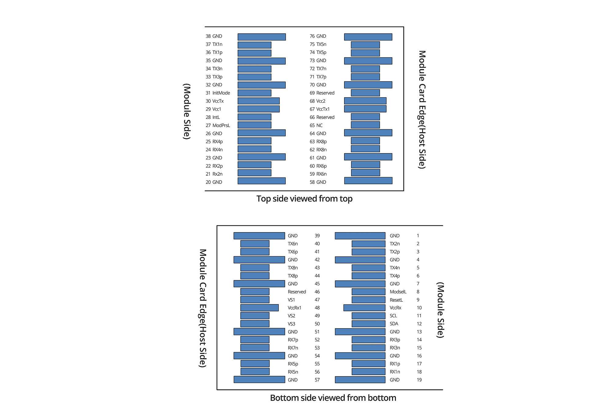
| Pin | Logic | Symbol | Description | Note | |||||
| 1 | – | GND | Ground | 1 | |||||
| 2 | CML-I | Tx2n | Transmitter Inverted Data Input | – | |||||
| 3 | CML-I | Tx2p | Transmitter Non-Inverted Data Input | – | |||||
| 4 | – | GND | Ground | 1 | |||||
| 5 | CML-I | Tx4n | Transmitter Inverted Data Input | – | |||||
| 6 | CML-I | Tx4p | Transmitter Non-Inverted Data Input | – | |||||
| 7 | – | GND | Ground | 1 | |||||
| 8 | LVTTL-I | ModSelL | Module Select | – | |||||
| 9 | LVTTL-I | ResetL | Module Reset | – | |||||
| 10 | – | VccRx | +3.3V Power Supply Receiver | 2 | |||||
| 11 | LVCOMS-I/O | SCL | 2-wire Serial Interface Clock | – | |||||
| 12 | LVCOMS-I/O | SDA | 2-wire Serial Interface Data | – | |||||
| 13 | – | GND | Ground | 1 | |||||
| 14 | CML-O | Rx3p | Receiver Non-Inverted Data Output | – | |||||
| 15 | CML-O | Rx3n | Receiver Inverted Data Output | – | |||||
| 16 | – | GND | Ground | 1 | |||||
| 17 | CML-O | GND | Ground | – | |||||
| 18 | CML-O | Rx1p | Receiver Non-Inverted Data Output | – | |||||
| 19 | – | GND | Ground | 1 | |||||
| 20 | – | GND | Ground | 1 | |||||
| 21 | CML-O | Rx2n | Receiver Inverted Data Output | – | |||||
| 22 | CML-O | Rx2p | Receiver Non-Inverted Data Output | – | |||||
| 23 | – | GND | Ground | 1 | |||||
| 24 | CML-O | Rx4n | Receiver Inverted Data Output | – | |||||
| 25 | CML-O | Rx4p | Receiver Non-Inverted Data Output | – | |||||
| 26 | – | GND | Ground | – | |||||
| 27 | LVTTL-O | ModPrsL | Module Present | – | |||||
| 28 | LVTTL-O | IntL | Interrupt | – | |||||
| 29 | – | VCCTx | +3.3 V Power Supply Transmitter | 2 | |||||
| 30 | – | VCC 1 | +3.3 V Power Supply | 2 | |||||
| 31 | LVTTL-I | InitMode | Initialization Mode; In Legacy QSFP Applications, the IntiMode Pad Is Called LPMode |
– | |||||
| 32 | – | GND | Ground | 1 | |||||
| 33 | CML-I | Tx3p | Transmitter Inverted Data Input | – | |||||
| 34 | CML-I | Tx3n | Transmitter Non-Inverted Data Output | – | |||||
| 35 | – | GND | Ground | 1 | |||||
| 36 | CML-I | Tx1p | Transmitter Inverted Data Input | – | |||||
| 37 | CML-I | Tx1n | Transmitter Non-Inverted Data Output | – | |||||
| 38 | – | GND | Ground | 1 | |||||
| 39 | – | GND | Ground | 1 | |||||
| 40 | CML-I | Tx6n | Transmitter Inverted Data Input | – | |||||
| 41 | CML-I | Tx6p | Transmitter Non-Inverted Data Output | – | |||||
| 42 | – | GND | Ground | 1 | |||||
| 43 | CML-I | Tx8n | Transmitter Inverted Data Input | – | |||||
| 44 | CML-I | Tx8p | Transmitter Non-Inverted Data Output | – | |||||
| 45 | – | GND | Ground | 1 | |||||
| 46 | – | Reserved | For Future Use | 3 | |||||
| 47 | – | VS1 | Module Vendor Specific 1 | 3 | |||||
| 48 | – | VCCRxx1 | +3.3V Power Supply Receiver | 2 | |||||
| 49 | – | VS2 | Module Vendor Specific 2 | 3 | |||||
| 50 | – | VS3 | Module Vendor Specific 3 | 3 | |||||
| 51 | – | GND | Ground | 1 | |||||
| 52 | CML-O | Rx7p | Receiver Non-Inverted Data Output | – | |||||
| 53 | CML-O | Rx7n | Receiver Inverted Data Output | – | |||||
| 54 | – | GND | Ground | 1 | |||||
| 55 | CML-O | Rx5p | Receiver Non-Inverted Data Output | – | |||||
| 56 | CML-O | Rx5n | Receiver Inverted Data Output | – | |||||
| 57 | – | GND | Ground | 1 | |||||
| 58 | – | GND | Ground | 1 | |||||
| 59 | CML-O | Rx6n | Receiver Inverted Data Output | – | |||||
| 60 | CML-O | Rx6p | Receiver Non-Inverted Data Output | – | |||||
| 61 | – | GND | Ground | 1 | |||||
| 62 | CML-O | Rx8n | Receiver Inverted Data Output | – | |||||
| 63 | CML-O | Rx8p | Receiver Non-Inverted Data Output | – | |||||
| 64 | – | GND | Ground | 1 | |||||
| 65 | – | NC | Not Connect | 3 | |||||
| 66 | – | Reserved | For Future Use | 3 | |||||
| 67 | – | VCCTx 1 | +3.3 V Power Supply Transmitter | 2 | |||||
| 69 | – | Reserved | For Future Use | 3 | |||||
| 70 | – | GND | Ground | 1 | |||||
| 71 | CML-I | Tx7p | Transmitter Inverted Data Input | – | |||||
| 72 | CML-I | Tx7n | Transmitter Non-Inverted Data Output | – | |||||
| 73 | – | GND | Ground | 1 | |||||
| 74 | CML-I | Tx5p | Transmitter Inverted Data Input | – | |||||
| 75 | CML-I | Tx5n | Transmitter Non-Inverted Data Output | – | |||||
| 76 | – | GND | Ground | 1 | |||||
| Note 1. QSFP-DD uses common ground (GND) for all signals and supply (power). All the common within the QSFP-DD module and all module voltages are referenced to this potential unless otherwise noted. Connected theses directly to the host board signal common ground plane.
Note 2. VCCRx, VCCRx1, VCC1, VCC2, VCCTx, and VCCTx1 shall be applied concurrently. Requirements defined for the host side of the Host Card Edge Connector are listed in Table 4. VCCRx, VCCRx1, VCC1, VCC2, VCCTx, and VCCTx1 may be internally connected within the module in any combination. The connector Vcc pins are each rated for a maximum current of 1000mA. Note 3. All Vendor Specific, Reserved and No Connect pins may be terminated with 50 ohms to ground on the host. Pad 65 (No Connect) shall be left unconnected within the module. Vendor Specific and Reserved pads shall have an impedance to GND that is greater than 10 kOhms and less than 100pF. |
|||||||||
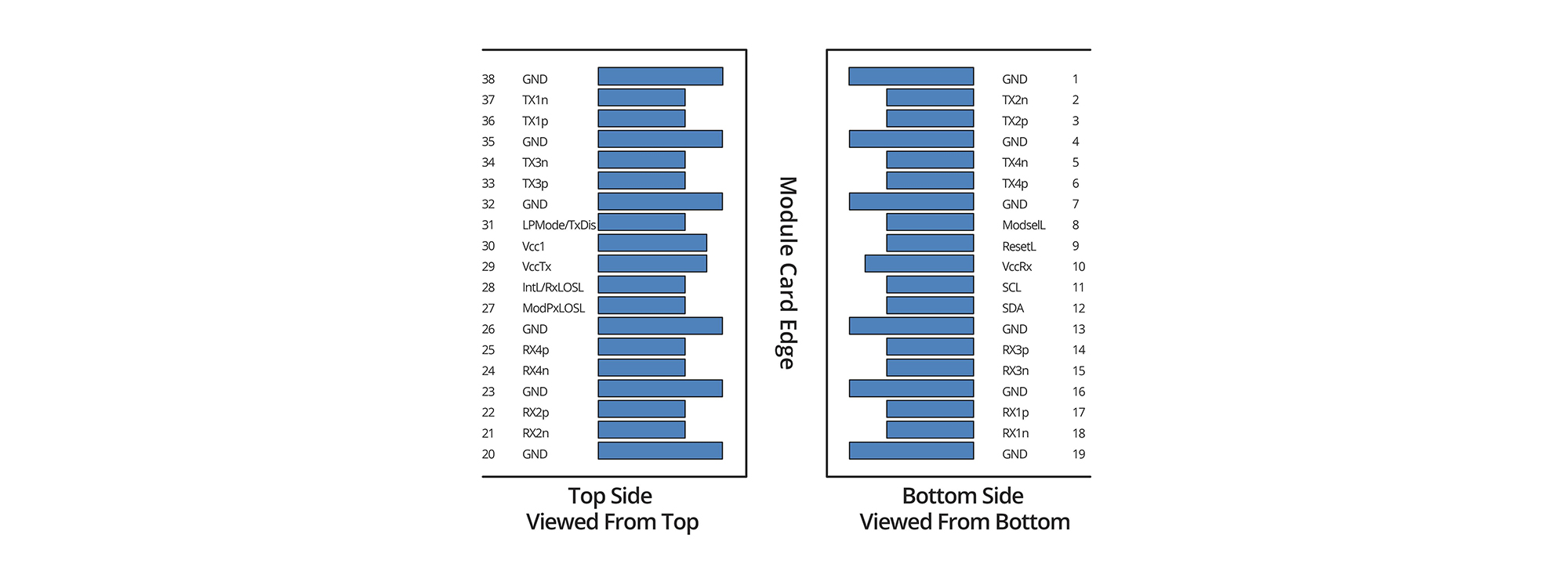
| Pin | Logic | Symbol | Description | Notes | |||||
| 1 | – | GND | Ground | 1 | |||||
| 2 | CML-I | Tx2n | Transmitter Inverted Data Input | – | |||||
| 3 | CML-I | Tx2p | Transmitter Non-inverted Data Input | – | |||||
| 4 | – | GND | Ground | 1 | |||||
| 5 | CML-I | Tx4n | Transmitter Inverted Data Input | – | |||||
| 6 | CML-I | Tx4p | Transmitter Non-Inverted Data Input | – | |||||
| 7 | – | GND | Ground | 1 | |||||
| 8 | LVTTL-I | ModSelL | Module Select | – | |||||
| 9 | LVTTL-I | ResetL | Module Reset | – | |||||
| 10 | – | VCC Rx | +3.3V Power Supply for Receiver | 2 | |||||
| 11 | LVTTL-I/O | SCL | 2-wire Serial Interface Clock | – | |||||
| 12 | LVTTL-I/O | SDA | – | – | |||||
| 13 | – | GND | – | 1 | |||||
| 14 | CML-O | Rx3p | – | – | |||||
| 15 | CML-O | Rx3n | – | – | |||||
| 16 | – | GND | – | 1 | |||||
| 17 | CML-O | Rx1p | – | – | |||||
| 18 | CML-O | Rx1n | – | – | |||||
| 19 | – | GND | – | 1 | |||||
| 20 | – | GND | – | 1 | |||||
| 21 | CML-O | Rx2n | – | – | |||||
| 22 | CML-O | Rx2p | – | – | |||||
| 23 | – | GND | – | 1 | |||||
| 24 | CML-O | Rx4n | – | – | |||||
| 25 | CML-O | Rx4p | – | – | |||||
| 26 | – | GND | – | 1 | |||||
| 27 | LVTTL-O | ModPrsL | – | – | |||||
| 28 | LVTTL-O | IntL/RxLOSL | – | – | |||||
| 29 | – | VCC Tx | – | 2 | |||||
| 30 | – | VCC1 | – | 2 | |||||
| 31 | LVTTL-I | LPMode | – | – | |||||
| 32 | – | GND | – | 1 | |||||
| 33 | CML-I | Tx3p | – | – | |||||
| 34 | CML-I | Tx3n | – | – | |||||
| 35 | – | GND | – | 1 | |||||
| 36 | CML-I | Tx1p | – | – | |||||
| 37 | CML-I | Tx1n | – | – | |||||
| 38 | – | GND | – | 1 | |||||
| Note1: GND is the symbol for signal and supply (power) common for the QSFP28 module. All are common within the module and all module voltages are referenced to this potential unless otherwise noted. Connect these directly to the host board signal common ground plane.
Note2: VccRx, Vcc 1 and VccTx are the receiving and transmission power suppliers and shall be applied concurrently.Recommended |
|||||||||

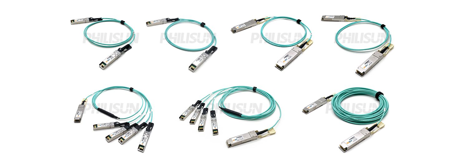
Related products
-

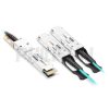
400G QSFP-DD to 8×50G SFP56 Active Optical Cable(AOC)
Compliant with QSFP-DD MSA/SFP28 MSA和IEEE 802.3cd standard
Switch to Switch
Switch to GPU -

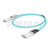
400G QSFP-DD to 4×100G QSFP28 Active Optical Cable(AOC)
Compliant with QSFP-DD MSA、SFF-8661、IEEE802.3bs-400GAUI-8、IEEE802.3bm-CAUI-4、CMIS 4.0、SFF-8636 standard
Switch to Switch
Switch to GPU -
")
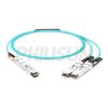
400G QSFP-DD to QSFP-DD Active Optical Cable (AOC)
Compliant with theSFF-8436 QSFP-DD MSA standard
Switch to Switch
Switch to GPU -

400G QSFP-DD to 4×100G QSFP56 Active Optical Cable(AOC)
Compliant with IEEE 802.3cd、OIF-CEI、QSFP-DD MSA、QSFP-DD-CMIS、IEEE 802.3bs Annex120E、SFF-8024、SFF-8679 standard
Switch to Switch
Switch to GPU