

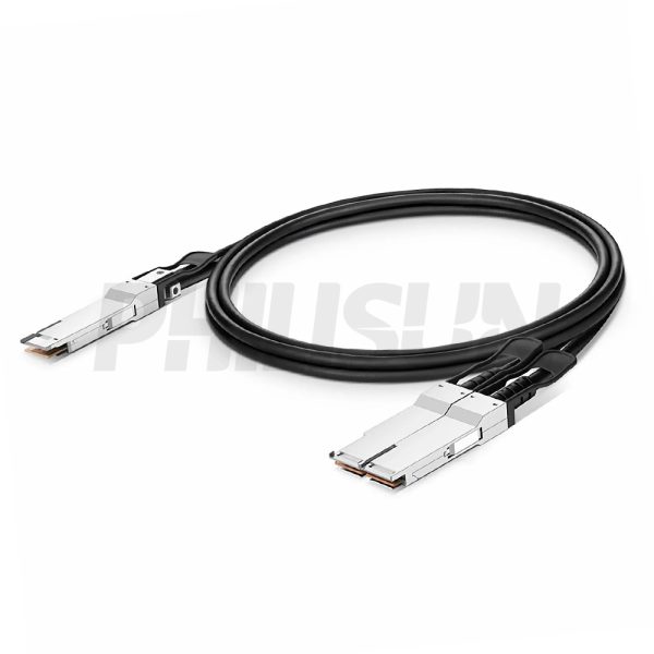
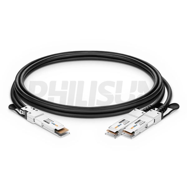
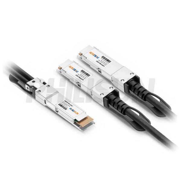

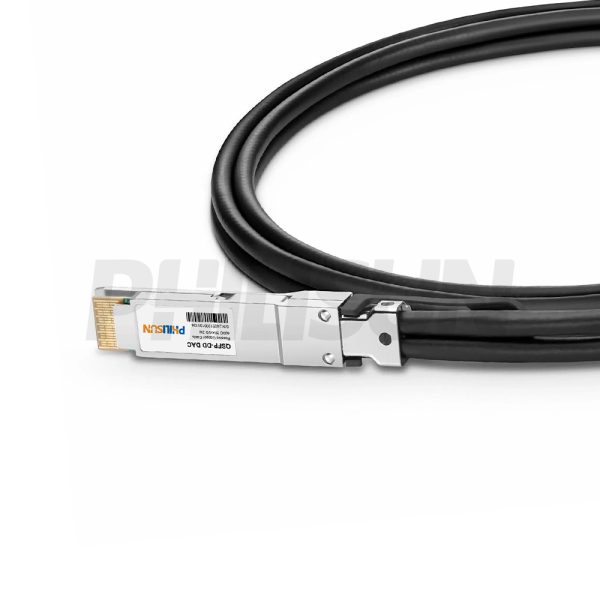
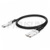
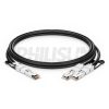
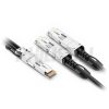
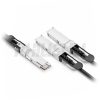
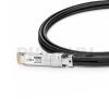
400G QSFP-DD to 2×200G QSFP56 Passive Direct Attach Copper Twinax Cable (DAC)
Compliant with SFF-8679、QSFP-DD MSA、IEEE802.3bj、IEEE802.3cd standard
Switch to Switch
Switch to GPU
- High Quality
- Factory Outlet
- Satisfaction Guarantee
- Global Shipping
| SPECIFICATIONS | |||
|---|---|---|---|
| Cable End Connector A | QSFP-DD | Cable End Connector B | 2×QSFP56 |
| Jumper Type | Active Optical Breakout Cable | Data Rate | 400G |
| Aggregate Bit Rate | 400Gbps | Lane Bit Rate | 50Gbps |
| Number of Channels | 8 | Single Channel Rate | 50G |
| Minimum Bend Radius | 5X Cable OD -Single, 10X Cable OD - Repeated | Factory Brand | PHILISUN |
| Attenuation | 28AWG:10dB/7m maximum 30AWG:8.4dB/5.5m maximum | Bit Error Rate | ≤10-12 |
| Shield | Braid/Foil | Wire AWG | 28AWG/30AWG |
| Cable Type | Passive Twinax | Cable OD | 30AWG: 6.7mm 28AWG: 7.9mm |
| Cable Colour/Material | Black PVC(OFNR) | Cable Length Selection | 0.5-3meter |
| Protocols | IEEE802.3Bj, By/IEEE802.3CD/QSFP-DD MSA/SFF-8636/SFF-8679 | Application Scenarios | 400Gigabit Ethernet (400GbE) |
| Supply Voltage | 3.3V | Power Dissipation | <0.1W |
| Operating Temperature | 0 to 70℃ (32 to 158℉) | Storage Temperature | -40 to 85℃ (-40 to 185℉) |
PRODUCT PRESENTATION
The PHILISUN 400G QSFP-DD to 2x200G QSFP56 Passive Direct Attach Copper Twinax Cable (DAC) is a flexible Breakout Cable designed for High-Density network segmentation, converting a single 400G port into two 200G QSFP56 channels. It is fully compliant with the QSFP-DD MSA, IEEE 802.3bj, and IEEE 802.3cd standard. This Passive Copper solution offers the lowest power consumption and Low Latency, making it a highly Cost-Effective link for Data Center architectures, supporting scalable Switch to Switch aggregation and high-throughput connections from Switch to GPU systems.
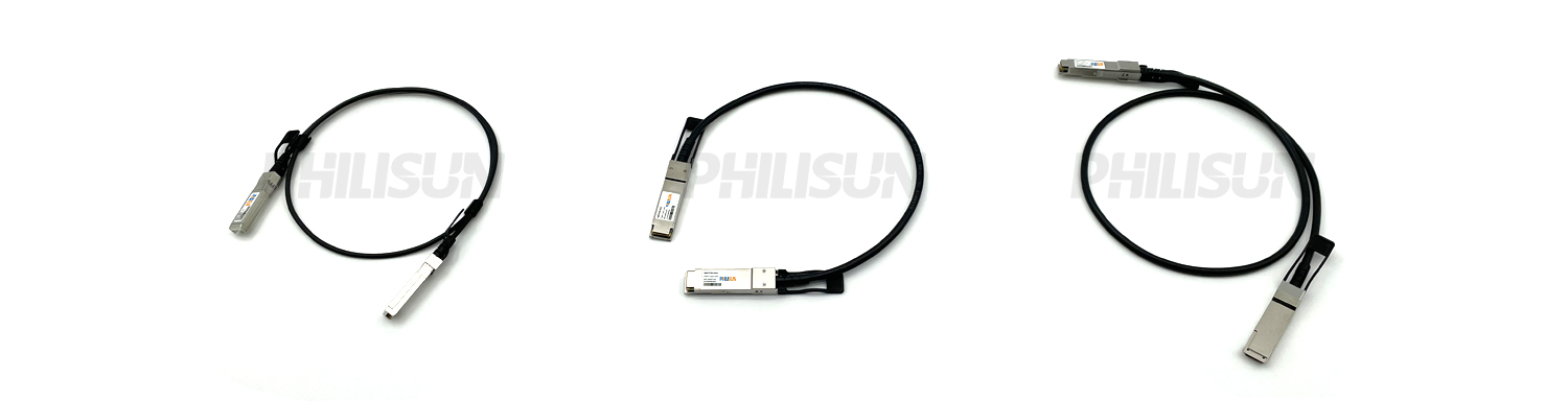
DAC SERIES PRODUCTS
PRODUCTION & TESTING EQUIPMENT

QSFP-DD Pin Define
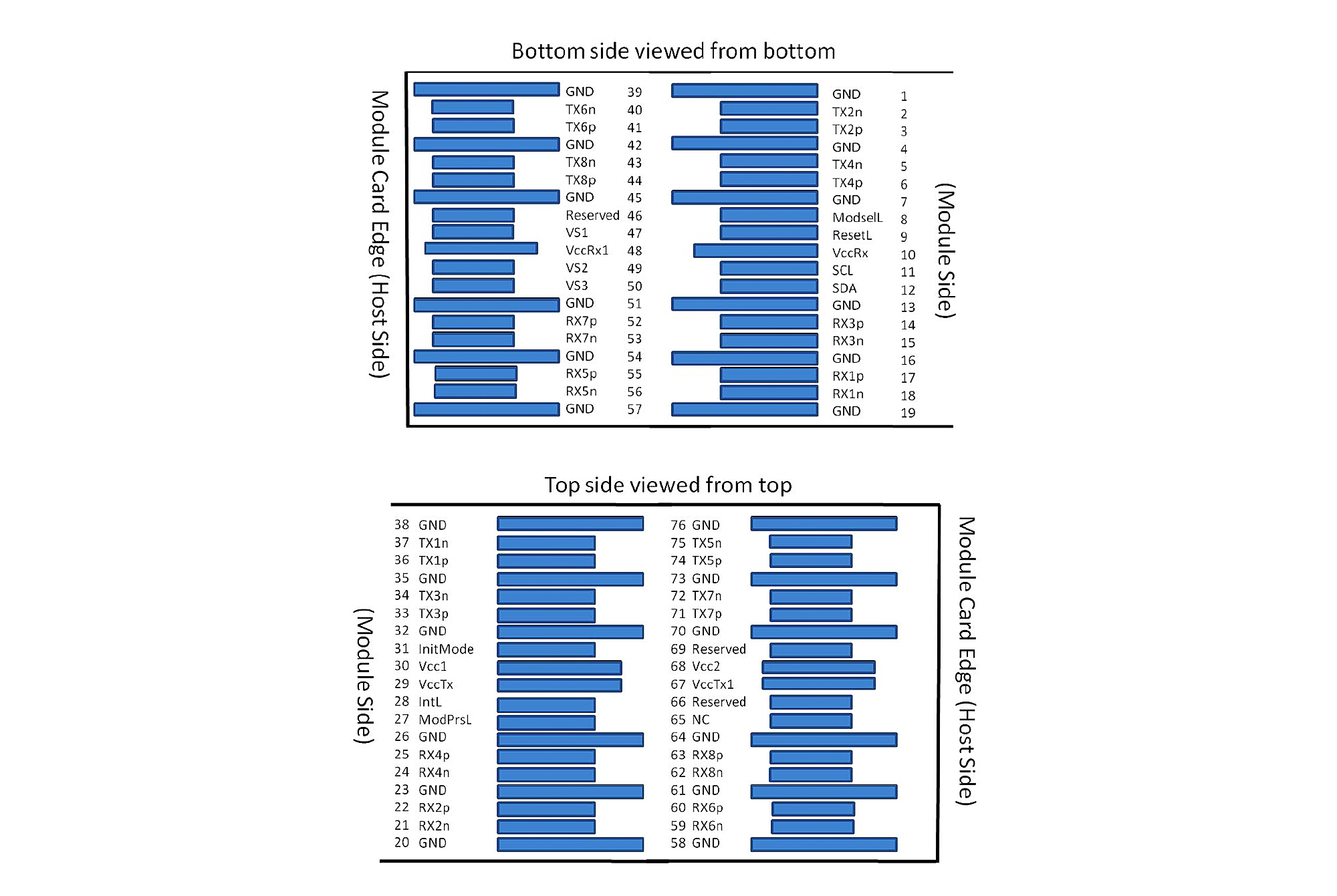
Pin Designation
| Pin | Logic | Symbol | Name/Description | Notes | |||||
| 1 | – | GND | Ground | 1 | |||||
| 2 | CML-I | Tx2n | Transmitter Inverted Data Input | – | |||||
| 3 | CML-I | Tx2p | Transmitter Non-Inverted Data Input | – | |||||
| 4 | – | GND | Ground | 1 | |||||
| 5 | CML-I | Tx4n | Transmitter Inverted Data Input | – | |||||
| 6 | CML-I | Tx4p | Transmitter Non-Inverted Data Input | – | |||||
| 7 | – | GND | Ground | 1 | |||||
| 8 | LVTTL-I | ModSelL | Module Select | – | |||||
| 9 | LVTTL-I | ResetL | Module Reset | – | |||||
| 10 | – | VccRx | +3.3V Power Supply Receiver | 2 | |||||
| 11 | LVCMOS-I/O | SCL | 2-wire serial interface clock | – | |||||
| 12 | LVCMOS-I/O | SDA | 2-wire serial interface data | – | |||||
| 13 | – | GND | Ground | 1 | |||||
| 14 | CML-O | Rx3p | Receiver Non-Inverted Data Output | – | |||||
| 15 | CML-O | Rx3n | Receiver Inverted Data Output | – | |||||
| 16 | – | GND | Ground | 1 | |||||
| 17 | CML-O | Rx1p | Receiver Non-Inverted Data Output | – | |||||
| 18 | CML-O | Rx1n | Receiver Inverted Data Output | – | |||||
| 19 | – | GND | Ground | 1 | |||||
| 20 | – | GND | Ground | 1 | |||||
| 21 | CML-O | Rx2n | Receiver Inverted Data Output | – | |||||
| 22 | CML-O | Rx2p | Receiver Non-Inverted Data Output | – | |||||
| 23 | – | GND | Ground | 1 | |||||
| 24 | CML-O | Rx4n | Receiver Inverted Data Output | – | |||||
| 25 | CML-O | Rx4p | Receiver Non-Inverted Data Output | – | |||||
| 26 | – | GND | Ground | 1 | |||||
| 27 | LVTTL-O | ModPrsL | Module Present | – | |||||
| 28 | LVTTL-O | IntL | Interrupt | – | |||||
| 29 | – | VccTx | +3.3V Power Supply Transmitter | 2 | |||||
| 30 | – | Vccl | +3.3V Power Supply | 2 | |||||
| 31 | LVTTL-I | InitMode | Initialization mode; In legacy QSFP applications, the InitMode pad is called LPMODE |
– | |||||
| 32 | – | GND | Ground | 1 | |||||
| 33 | CML-I | Tx3p | Transmitter Non-Inverted Data Input | – | |||||
| 34 | CML-I | Tx3n | Transmitter Inverted Data Input | – | |||||
| 35 | – | GND | Ground | 1 | |||||
| 36 | CML-I | Tx1p | Transmitter Non-Inverted Data Input | – | |||||
| 37 | CML-I | Tx1n | Transmitter Inverted Data Input | – | |||||
| 38 | – | GND | Ground | 1 | |||||
| 39 | – | GND | Ground | 1 | |||||
| 40 | CML-I | Tx6n | Transmitter Inverted Data Input | – | |||||
| 41 | CML-I | Tx6p | Transmitter Non-Inverted Data Input | – | |||||
| 42 | – | GND | Ground | 1 | |||||
| 43 | CML-I | Tx8n | Transmitter Inverted Data Input | – | |||||
| 44 | CML-I | Tx8p | Transmitter Non-Inverted Data Input | – | |||||
| 45 | – | GND | Ground | 1 | |||||
| 46 | – | Reserved | For future use | 3 | |||||
| 47 | – | VSl | Module Vendor Specific 1 | 3 | |||||
| 48 | – | VccRx1 | 3.3V Power Supply | 3 | |||||
| 49 | – | VS2 | Module Vendor Specific 2 | 3 | |||||
| 50 | – | VS3 | Module Vendor Specific 3 | 3 | |||||
| 51 | – | GND | Ground | 1 | |||||
| 52 | CML-O | Rx7p | Receiver Non-Inverted Data Output | – | |||||
| 53 | CML-O | Rx7n | Receiver Inverted Data Output | – | |||||
| 54 | – | GND | Ground | 1 | |||||
| 55 | CML-O | Rx5p | Receiver Non-Inverted Data Output | – | |||||
| 56 | CML-O | Rx5n | Receiver Inverted Data Output | – | |||||
| 57 | – | GND | Ground | 1 | |||||
| 58 | – | GND | Ground | 1 | |||||
| 59 | CML-O | Rx6n | Receiver Inverted Data Output | – | |||||
| 60 | CML-O | Rx6p | Receiver Non-Inverted Data Output | – | |||||
| 61 | – | GND | Ground | 1 | |||||
| 62 | CML-O | Rx8n | Receiver Inverted Data Output | – | |||||
| 63 | CML-O | Rx8p | Receiver Non-Inverted Data Output | – | |||||
| 64 | – | GND | Ground | 1 | |||||
| 65 | – | NC | No Connect | 3 | |||||
| 66 | – | Reserved | For future use | 3 | |||||
| 67 | – | VccTx1 | 3.3V Power Supply | 2 | |||||
| 68 | – | Vcc2 | 3.3V Power Supply | 2 | |||||
| 69 | – | Reserved | For future use | 3 | |||||
| 70 | – | GND | Ground | 1 | |||||
| 71 | CML-I | Tx7p | Transmitter Non-Inverted Data Input | – | |||||
| 72 | CML-I | Tx7n | Transmitter Inverted Data Input | – | |||||
| 73 | – | GND | Ground | 1 | |||||
| 74 | CML-I | Tx5p | Transmitter Non-Inverted Data Input | – | |||||
| 75 | CML-I | Tx5n | Transmitter Inverted Data Input | – | |||||
| 76 | – | GND | Ground | 1 | |||||
| Notes: 1. QSFP-DD TO 2 QSFP56 uses common ground (GND)for all signals and supply (power). All are common within the QSFP-DD TO 2 QSFP56 module and all module voltages are referenced to this potential unless otherwise noted. Connect these directly to the host board signal-common ground plane. 2. VccRx, VccRx1, Vcc1, Vcc2, VccTx and VccTx1 shall be applied concurrently. Requirements defined for the host side of the Host Card Edge Connector are listed in Table 6. VccRx, VccRx1, Vcc1, Vcc2, VccTx and VccTx1 may be internally connected within the module in any combination. The connector Vcc pins are each rated for a maximum current of 1000 mA. 3. All Vendor Specific, Reserved and No Connect pins may be terminated with 50 ohms to ground on the host. Pad 65 (No Connect) shall be left unconnected within the module. Vendor specific and Reserved pads shall have an impedance to GND that is greater than 10 kOhms and less than 100 pF. 4. Plug Sequence specifies the mating sequence of the host connector and module. The sequence is 1A, 2A, 3A, 1B, 2B, 3B. (see Figure 2 for pad locations) Contact sequence A will make, then break contact with additional QSFP-DD TO 2 QSFP pads. Sequence 1A, 1B will then occur simultaneously, followed by 2A, 2B, followed by 3A,3B. |
|||||||||
2-Wires EEPROM Interface
| A0h address | Name | Value | Description | ||||||
| 0 | Identifier | 18 | Type of Serial Module — See SFF-8024,19h:OSFP 8X | ||||||
| 1 | Version ID | 30 | the upper nibble is the whole number part andthe lower nibble is the decimal part.Example: 21h |
||||||
| 2 | Flat_mem | 80 | Upper memory flat or paged.0b=Paged memory 1b=Flat memory (only page 00h implemented) |
||||||
| CLEI present | |||||||||
| Reserved Reserved | CLEI code present in upper page 00h | ||||||||
| TWI Maximum speed | Reserved | ||||||||
| Reserved | Reserved | ||||||||
| 3 | Reserved | 03 | Reserved | ||||||
| Module state | Current state of Module 001b:ModuleLowPwr state(Flat memory passive cable assemblies) |
||||||||
| Interrupt | Digital state ofIntL Interrupt output signal0b=IntL asserted1b=IntL not asserted (default) |
||||||||
| 4~7 | Bank 0 lane flag | 00 | Indicates that one or more of the flag bits from bank 0 | ||||||
| 8 | Reserved | 00 | Module state changed flag | ||||||
| Reserved | Indicates change of Module state | ||||||||
| 9~13 | Module Interrupt Flags | 00 | Module Interrupt Flags | ||||||
| 14~25 | Module monitors | 00 | Module monitors Temperature MSB | ||||||
| 26~30 | Module Global Controls | 00 | ForceLowPwr,Software Reset,Custom | ||||||
| 31~36 | Module Level Flag Masks | 00 | Module Level Flag Masks | ||||||
| 37~63 | Reserved | 00 | Reserved | ||||||
| 64~84 | Custom | 00 | Custom | ||||||
| 85 | Module Type Encodings | 03 | 00h:Undefined01h:Optical Interfaces: MMF 02h:Optical interfaces: SMF 03h:Passive Cu 04h:Active Cable 005:Base-T |
||||||
| 86 | Module Host Electrical interface codes(ApSel:0001b) |
1D | 1A:100GBASE-CR4 NRZ 1D:400G CR8 PAM4 |
||||||
| 87 | Module Media interface codes(ApSel:0001b) |
01 | 01:Copper cable | ||||||
| 88 | Host/Media Lane Count(ApSel:0001b) |
88 | 7-4:Host Lane Count 3-0:Media Lane Count |
||||||
| 89 | Lane Assignment(ApSel:0001b) |
00 | code 1:if application is allowed on a given host lane.bits0-7 correspond to host lanes 1-8 |
||||||
| 90 | Module Host Electrical interface codes(ApSel:0010b) |
00 | Module Host-Media Interface Advertising Codes | ||||||
| 91 | Module Media interface codes(ApSel:0010b) |
00 | Module Host-Media Interface Advertising Codes | ||||||
| 92 | Host/Media Lane Count(ApSel:0010b) |
00 | Module Host-Media Interface Advertising Codes | ||||||
| 93 | Lane Assignment(ApSel:0010b) |
00 | Module Host-Media Interface Advertising Codes | ||||||
| 94 | Module Host Electrical interface codes(ApSel:0011b) |
00 | Module Host-Media Interface Advertising Codes | ||||||
| 95 | Module Media interface codes(ApSel:0011b) |
00 | Module Host-Media Interface Advertising Codes | ||||||
| 96 | Host/Media Lane Count(ApSel:0011b) |
00 | Module Host-Media Interface Advertising Codes | ||||||
| 97 | Lane Assignment(ApSel:0011b) |
00 | Module Host-Media Interface Advertising Codes | ||||||
| 98 | Module Host Electrical interface codes(ApSel:0100b) |
00 | Module Host-Media Interface Advertising Codes | ||||||
| 99 | Module Media interface codes(ApSel:0100b) |
00 | Module Host-Media Interface Advertising Codes | ||||||
| 100 | Host/Media Lane Count(ApSel:0100b) |
00 | Module Host-Media Interface Advertising Codes | ||||||
| 101 | Lane Assignment(ApSel:0100b) |
00 | Module Host-Media Interface Advertising Codes | ||||||
| 102 | Module Host Electrical interface codes(ApSel:0101b) |
00 | Module Host-Media Interface Advertising Codes | ||||||
| 103 | Module Media interface codes(ApSel:0101b) |
00 | Module Host-Media Interface Advertising Codes | ||||||
| 104 | Host/Media Lane Count(ApSel:0101b) |
00 | Module Host-Media Interface Advertising Codes | ||||||
| 105 | Lane Assignment(ApSel:0101b) |
00 | Module Host-Media Interface Advertising Codes | ||||||
| 106 | Module Host Electrical interface codes(ApSel:0110b) |
00 | Module Host-Media Interface Advertising Codes | ||||||
| 107 | Module Media interface codes(ApSel:0110b) |
00 | Module Host-Media Interface Advertising Codes | ||||||
| 108 | Host/Media Lane Count(ApSel:0110b) |
00 | Module Host-Media Interface Advertising Codes | ||||||
| 109 | Lane Assignment(ApSel:0110b) |
00 | Module Host-Media Interface Advertising Codes | ||||||
| 110 | Module Host Electrical interface codes(ApSel:0111b) |
00 | Module Host-Media Interface Advertising Codes | ||||||
| 111 | Module Media interface codes(ApSel:0111b) |
00 | Module Host-Media Interface Advertising Codes | ||||||
| 112 | Host/Media Lane Count(ApSel:0111b) |
00 | Module Host-Media Interface Advertising Codes | ||||||
| 113 | Lane Assignment(ApSel:0111b) |
00 | Module Host-Media Interface Advertising Codes | ||||||
| 114 | Module Host Electrical interface codes(ApSel:1000b) |
00 | Module Host-Media Interface Advertising Codes | ||||||
| 115 | Module Media interface codes(ApSel:1000b) |
00 | Module Host-Media Interface Advertising Codes | ||||||
| 116 | Host/Media Lane Count(ApSel:1000b) |
00 | Module Host-Media Interface Advertising Codes | ||||||
| 117 | Lane Assignment(ApSel:1000b) |
00 | Module Host-Media Interface Advertising Codes | ||||||
| 118~125 | Password Entry and Change | 00 | Password Entry and Change | ||||||
| 126 | Bank Select Byte | 00 | The module shall ignore the Bank Select byte if the Page Select byte is outside of the 10h to 1Fh range (inclusive).In this case the Bank Select byte shall revert to bank 0 and read/write operations shall be to bank 0. |
||||||
| 127 | Page Select Byte | 00 | Writing the value of a non-supported page shall not be accepted by the module. In such cases the Page Select byte shall revert to 0 and read/write operations shall be to upper page 00h. |
||||||
| 128 | Identifier | 18 | Identifier Type of Module | ||||||
| 129~144 | Vendor name | * | Vendor name(ASCII) | ||||||
| 145 | Vendor OUI | 3C | Vendor IEEE company ID | ||||||
| 146 | – | 18 | – | ||||||
| 147 | – | A0 | – | ||||||
| 148~163 | Vendor PN | * | Part number provided by vendor(ASCII) | ||||||
| 164 | Vendor rev | 41 | Vendor rev A | ||||||
| 165 | – | 20 | Vendor rev A | ||||||
| 200 | Module Card Power Class | 00 | 000: Power class 1; 001: Power class 2010: Power class 3; 011: Power class 4100: Power class 5; 101: Power class 6110: Power class 7; 111: Power class 8 |
||||||
| 201 | Max Power | 06 | Maximum power consumption in multiples of 0.25 W rounded up to the next whole multiple of 0.25 W |
||||||
| 202 | Cable assembly Length Lenth multiplier field
Cable assembly Length Base Length field |
* | Multiplier for value in bits 5-0.00 = multiplier of .101 = multiplier of 110 = multiplier of 1011 = multiplier of 100 Link length base value. To calculate actual link length |
||||||
| 203 | Media connector Type | 23 | Type of connector present in the module.See SFF- 8024 for codes.23h:Non-separable Connector |
||||||
| 204 | Copper cable Attenuation 5GHz | * | Passive copper cable attenuation at 5 GHz in 1 dB increments |
||||||
| 205 | Copper cable Attenuation 7GHz | * | Passive copper cable attenuation at 7 GHz in 1 dB increments |
||||||
| 206 | Copper cable Attenuation 12.89GHz | * | Passive copper cable attenuation at 12.89 GHz in 1 dB increments |
||||||
| 207 | Copper cable Attenuation 25.8GHz | * | Passive copper cable attenuation at 25.8 GHz in 1 dB increments |
||||||
| 208 | Reserved | 00 | Reserved | ||||||
| 209 | Reserved | 00 | Reserved | ||||||
| 210 | Near end implementation lane 8 | 00 | 0b=Lane 8 implemented in near end1b=Lane 8 not implemented in near end |
||||||
| 211 | Reserved
Implemented lanes in far end |
02 | Reserved
See Table 27 for config code of discrete far end |
||||||
| 212 | Media interface technology | 0A | 0A: Copper cable unequalized | ||||||
| 213~220 | Reserved | 00 | Reserved | ||||||
| 221 | Custom | 00 | Custom | ||||||
| 222 | Checksum | * | Include bytes 128-221 | ||||||
| 223~251 | User custom info NV | 00 | User custom info NV | ||||||
| 252~255 | User custom info NV | 00 | User custom info NV | ||||||
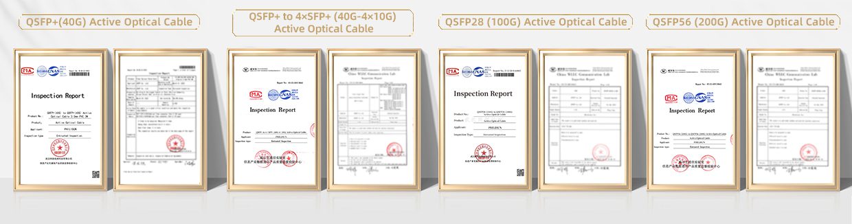
PRODUCT CERTIFICATION
COMPATIBLE BRANDS

CONFIGURATION INFORMATION
Related products
-

400G QSFP-DD to 4×100G QSFP56 Passive Direct Attach Copper Twinax Cable (DAC)
Compliant with SFF-8665、QSFP-DD MSA、IEEE802.3bj、IEEE802.3cd standard
Switch to Switch
Switch to GPU -

400G QSFP-DD to 8×50G SFP56 Passive Direct Attach Copper Twinax Cable (DAC)
Compliant with QSFP-DD MSA、SFF-8432、IEEE 802.3bs-400GAUI-8、IEEE802.3cd-50GAUI-1、CMIS 4.0、SFF-8472 standard
Switch to Switch
Switch to GPU -

400G QSFP-DD to QSFP-DD Passive Direct Attach Copper Twinax Cable (DAC)
Compliant with IEEE 802.3cd, QSFP-DD MSA, CMIS 4.0 standard
Switch to Switch
Switch to GPU