

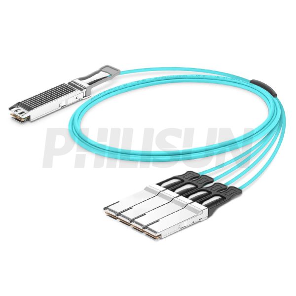
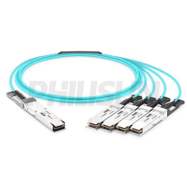
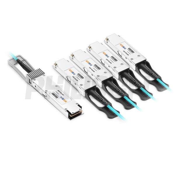
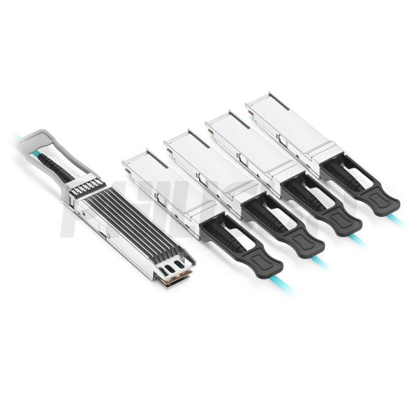
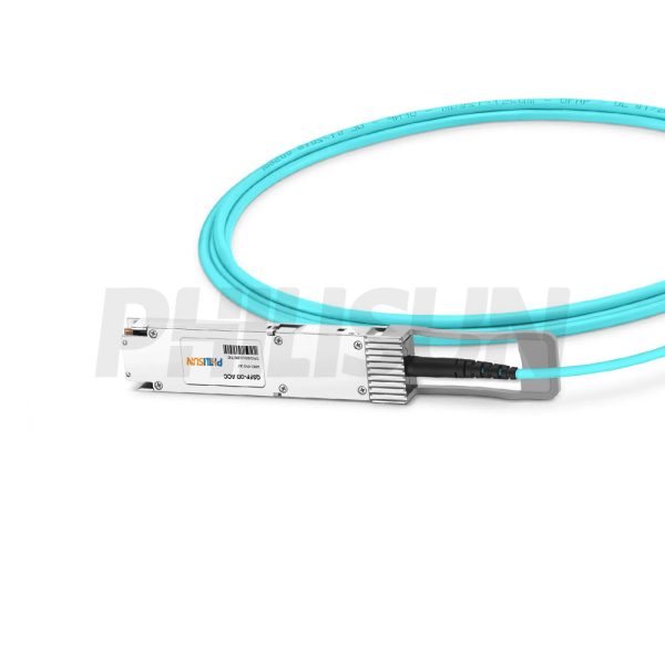
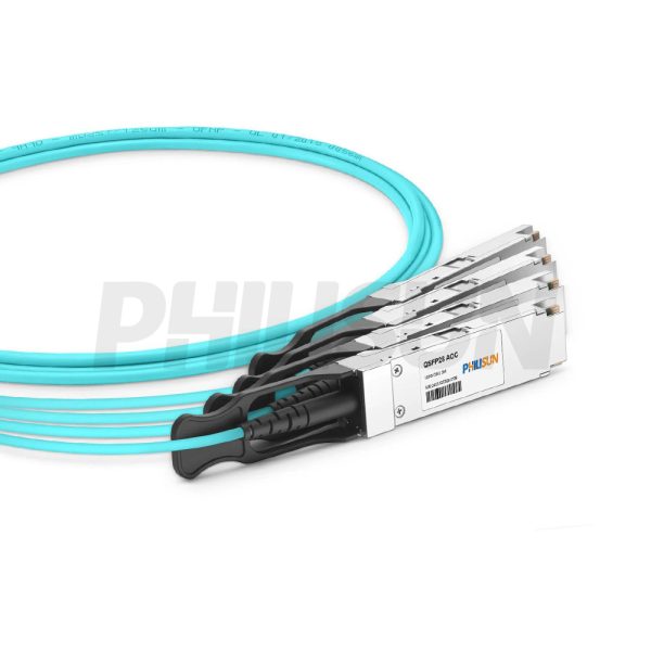

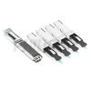


400G QSFP-DD to 4×100G QSFP28 Active Optical Cable(AOC)
Compliant with QSFP-DD MSA、SFF-8661、IEEE802.3bs-400GAUI-8、IEEE802.3bm-CAUI-4、CMIS 4.0、SFF-8636 standard
Switch to Switch
Switch to GPU
- High Quality
- Factory Outlet
- Satisfaction Guarantee
- Global Shipping
| SPECIFICATIONS | |||
|---|---|---|---|
| Cable End Connector A | QSFP-DD | Cable End Connector B | 4×QSFP28 |
| Jumper Type | Active Optical Breakout Cable | Data Rate | 400G |
| Aggregate Bit Rate | 425Gbps | Lane Bit Rate | 53.125Gbps |
| Number of Channels | 8 | Single Channel Rate | 50G |
| Array Transmitter | VSCEL | Array Receiver | PIN |
| Minimum Bend Radius | 30mm | Factory Brand | PHILISUN |
| Center(Operating) Wavelength | 850nm | Bit Error Rate | 2.4E-4 |
| Fiber Type | OM3 MMF MAX 70m/OM4 MMF MAX 100m | Cable Colour | Aqua |
| Cable Material | LSZH/OFNP | Cable Length Selection | 1-100meter |
| Safety Certification | TUV/UL/FDA | Application Scenarios | 400 Gigabit Ethernet (400GbE) |
| Protocols | SFF-8679/SFF-8661/QSFP-DD-CMIS-Rev4.0/SFF-8636/IEEE 802.3cd | DDMI(Commercial) | YES |
| Supply Voltage | 3.3V | Power Dissipation | QSFP-DD:<12.0W QSFP56:<3.5W |
| Operating Temperature | 0 to 70℃ (32 to 158℉) | Storage Temperature | -20 to 85℃ (-4 to 185℉) |

| General Product Characteristics | |||||||||
| Parameter | Value | Unit | Comments | ||||||
| Module Form Factor | QSFP-DD and QSFP | – | Module Form Factor | ||||||
| Number of Lanes | 8TXand8RX | – | – | ||||||
| Maximum Aggregate Data Rate | 425(QSFP-DD) 103. 1(QSFP) |
Gb/s | – | ||||||
| Maximum Data Rate per Lane | 53.125 | Gb/s | – | ||||||
| Standard Cable Lengths | 3, 5, 7, 10, 15, 20 | meters | Other lengths maybe available upon request | ||||||
| Electrical Interface and Pin- out | 76-pin edge connector (QSFP-DD) 38-pin edge connector(QSFP28) | – | Pin-out as defined byQSFP-DD Rev 4.0 & QSFPSFF8679 | ||||||
| Maximum Power Consumption per End | 12(QSFP-DD)and 3.5(QSFP28) | Watts | Varies with output voltageswing and pre-emphasis settings | ||||||
| Force Specification | |||||||||
| Parameter | Min. | Max. | Unit. | Comments. | |||||
| Module Insertion | – | 90(QSFP-DD) 40(QSFP28) |
Newton | – | |||||
| ModuleExtraction | – | 50(QSFP-DD) 30(QSFP28) |
Newton | – | |||||
| Module Retention | 90(QSFP-DD) 90(QSFP28) |
– | Newton | – | |||||
| Insertion and removalcycles | 50 | – | Cycle | – | |||||
| Mechanical Specification | |||||||||
| Parameter | Symbol | Min. | Typ. | Max. | Unit. | Ref. | |||
| Maximum Supply Voltage | Vcc | -0.5 | – | 3.6 | V | – | |||
| Storage Temperature | Tsto | -40 | – | 85 | ℃ | – | |||
| Case Operating Temperature | Top_1 | 0 | – | 60 | ℃ | ① 、② | |||
| Top_2 | 0 | – | 70 | ℃ | ② | ||||
| Relative Humidity | RH | 5 | – | 85 | % | – | |||
| 1.DDMI temperature reading is measured by the position of Top_1 2.Case operating temperature definition: |
|||||||||
| Recommended Operating Environment | |||||||||
| Parameter | Symbol | Min. | Typ. | Max. | Unit. | Ref. | |||
| Supply Voltage | Vcc | 3.14 | – | 3.46 | V | – | |||
| Power Consumption | PCon | – | – | 12(QSFP-DD) 3.5(QSFP28) |
W | – | |||
| Optical Data Rate (PAM4) | BR | – | 26.5625 | – | GBd | ① | |||
| Electrical Data Rate for QSFP28 (NRZ) |
BR | – | 25.78125 | – | Gb/s | – | |||
| Center wavelength | λc | 840 | – | 860 | nm | ② | |||
| Pre-FEC Bit Error Rate (PAM4) | – | – | – | 2.4×10⁻⁴ | – | ③ | |||
| Pre-FEC Bit Error Rate (NRZ) | – | – | – | 5×10⁻⁵ | – | – | |||
| Parameter | Symbol | Min. | Typ. | Max. | Unit. | Ref. | |||
| Post-FEC Bit Error Rate | – | – | – | 1×10-12 | – | – | |||
| Beam divergence angle | – | – | 23 | – | ˚ | – | |||
| Number of Lanes | – | – | 8 | – | – | – | |||
| Management Interface | – | Serial, I2C-based,maximumfrequeny | 400kHz | – | ④ | ||||
| Logic Input Voltage High | Vih | 2 | – | Vcc+0.3 | V | – | |||
| Logic Input Voltage Low | Vil | -0.3 | – | 0.8 | V | – | |||
| ① Single lane ② PRBS31Q test pattern is used. ③ As defined by IEEE Std. 802.3bs ™/D3.5 ④ As defined by SFF-8636 |
|||||||||
| Electrical Characteristics | |||||||||
| Parameter | Symbol | Min. | Typ. | Max. | Unit. | Ref. | |||
| TransmitteratTP1a | |||||||||
| AC common-mode output voltage (RMS) | – | – | – | 17.5 | mV | ||||
| Differential peak-to-peak output voltage (Transmitterdisabled) |
– | – | – | 35 | mV | ||||
| Differential peak-to-peak output voltage (Transmitterenabled) |
– | – | – | 880 | mV | ||||
| Eye symmetry mask width | ESMW | – | 0.22 | – | UI | ||||
| Eyeheight,differential | EH | 32 | – | – | mV | ||||
| Differentia loutput returnloss | – | SeeEq.1 | – | – | – | ||||
| Common to differential mode conversion return loss | – | SeeEq. 2 | – | – | – | ||||
| Differential termination mismatch | – | 10 | – | – | % | ||||
| Transition time (20%to80%) | Tr,Tf | – | – | 10 | ps | ||||
| Receiverat TP4 | |||||||||
| Far-end Eye height,differential | – | 30 | – | – | mV | ||||
| Far-end pre-cursorISIratio | – | -4.5 | 2.5 | % | |||||
| Differential output return loss | – | SeeEq.1 | – | – | – | ||||
| Common to differential mode conversion return loss | – | SeeEq. 2 | – | – | – | ||||
| Differential ermination mismatch | – | 10 | – | – | % | ||||
| Parameter | Symbol | Min. | Typ. | Max. | Unit. | Ref. | |||
| Transitiontime(20%to80%) | Tr,Tf | 10 | – | – | ps | – | |||
| DCcommon modevoltage | – | -350 | – | 2850 | mV | – | |||
| TransmitteratTP1a | |||||||||
| Differential Data Output Voltage Peak to Peak Swing | Vin,pp | – | – | 900 | mV | – | |||
| Differential Input Return Loss | SDD22 | Per OIF CEI-28G-VSR and CAUI-4 Requirements |
dB | – | |||||
| Common Mode to Differential Conversion and Differential to Common Mode Conversion | SDD22 SCD22 |
dB | – | ||||||
| Common Mode Return Loss | SCC22 | dB | – | ||||||
| Transition Time,20% to 80% | Tr,Tf | 10 | – | – | ps | – | |||
| Common Mode Voltage | Vcm | -0.3 | – | 2.8 | V | – | |||
| Receiverat TP4 | |||||||||
| Differential Data Output Voltage Peak to Peak Swing | Vopp | 900 | mV | – | |||||
| Differential Output Impedance | Zos | 90 | 100 | 110 | Ohms | – | |||
| Common Mode Voltage | Vcm | -0.35 | 2.85 | V | ① | ||||
| Differential Output Return Loss | SDD22 | Per OIF CEI-28G-VSR and Requirements | CAUI-4 | dB | – | ||||
| Common Mode to Differential Conversion and Differential to Common Mode Conversion |
SDD22 SCD22 |
– | – | – | |||||
| Common Mode Return Loss | SCC22 | – | – | -2.00 | dB | ② | |||
| Transition Time,20% to 80% | Tr,Tf | 10 | – | – | ps | – | |||
| Eye Width @1E-15 Probability | EW15 | 0.57 | – | – | UI | – | |||
| Eye Height@1E-15P robability | EH15 | 228 | – | – | mV | – | |||
| ① Vcm is generated by the host. Specification includes effects of ground offset voltage. ② From 250MHz to 30GHz |
|||||||||
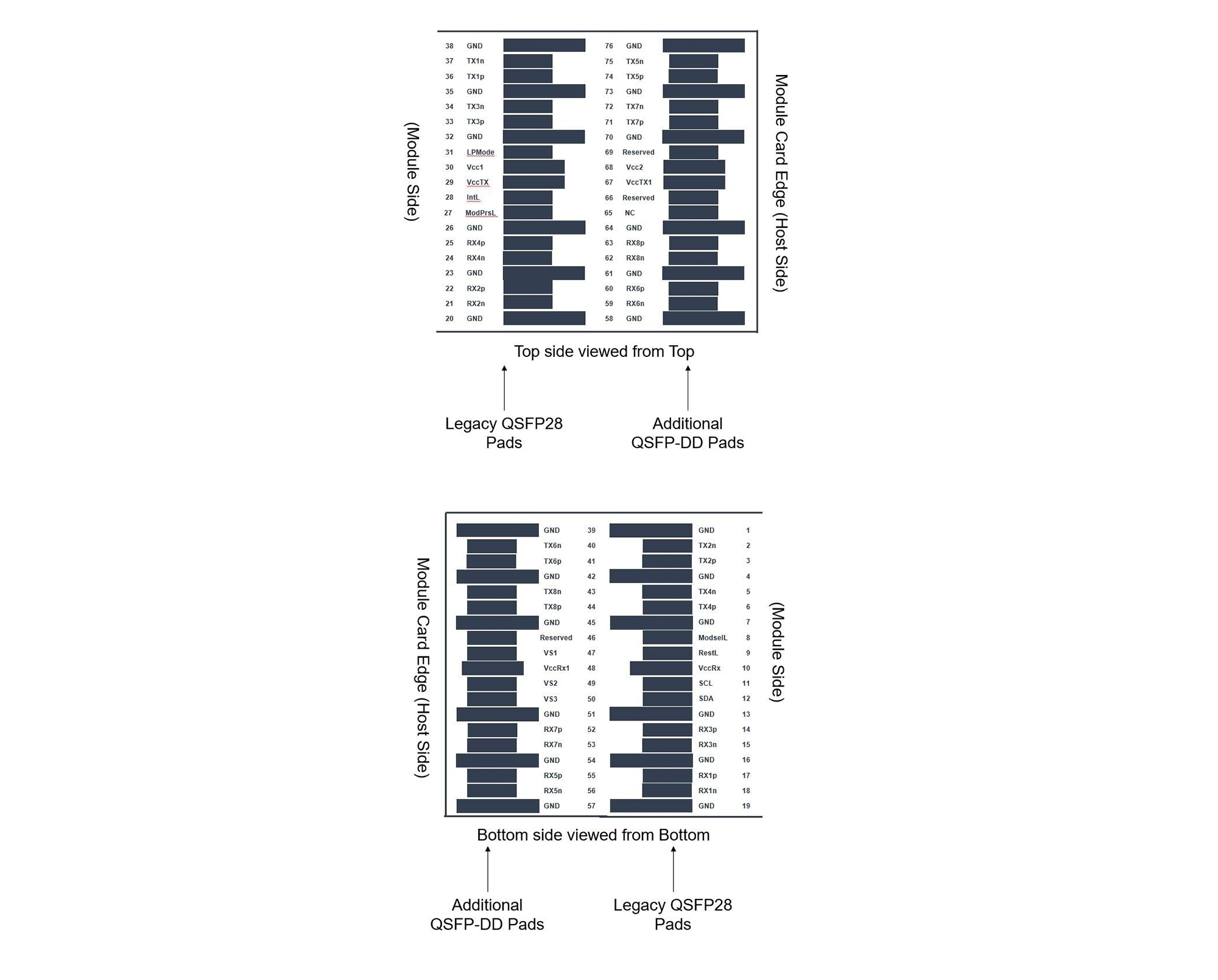
| PIN | Symbol | Description | Ref. | ||||||
| 1 | GND | Ground | ® | ||||||
| 2 | TX2n | Transmitter Inverted Data Input | – | ||||||
| 3 | TX2p | Transmitter Non-Inverted Data Input | – | ||||||
| 4 | GND | Ground | ® | ||||||
| 5 | TX4n | Transmitter Inverted Data Input | – | ||||||
| 6 | TX4p | Transmitter Non-Inverted Data Input | – | ||||||
| 7 | GND | Ground | ® | ||||||
| 8 | ModSelL | Module Select | – | ||||||
| 9 | ResetL | Module Reset | – | ||||||
| 10 | VccRX | +3.3VPower Supply Receiver | ® | ||||||
| 11 | SCL | 2-wire serial interface clock | – | ||||||
| 12 | SDA | 2-wire serial interface data | – | ||||||
| 13 | GND | Ground | ® | ||||||
| 14 | RX3p | ReceiverNon-Inverted Data Output | – | ||||||
| 15 | RX3n | Receiver Inverted Data Output | – | ||||||
| 16 | GND | Ground | ® | ||||||
| 17 | RX1p | Receiver Non-Inverted Data Output | – | ||||||
| 18 | RX1n | Receiver Inverted Data Output | – | ||||||
| 19 | GND | Ground | ® | ||||||
| 20 | GND | Ground | ® | ||||||
| 21 | RX2n | Receiver Inverted Data Output | – | ||||||
| 22 | RX2p | Receiver Non-Inverted Data Output | – | ||||||
| 23 | GND | Ground | ® | ||||||
| 24 | RX4n | Receiver Inverted Data Output | – | ||||||
| 25 | RX4p | Receiver Non-Inverted Data Output | – | ||||||
| 26 | GND | Ground | ® | ||||||
| 27 | ModPrsL | Module Present | – | ||||||
| 28 | IntL | Interrupt | – | ||||||
| 29 | VccTX | +3.3V Power supply transmitter | ® | ||||||
| 30 | Vcc1 | “+3.3V Powersupply | ® | ||||||
| 31 | LPMode | Initializationmode;Inlegacy QSFP applications, the InitMode pad is called LPMODE | – | ||||||
| 32 | GND | Ground | ® | ||||||
| 33 | TX3p | Transmitter Non-Inverted Data Input | – | ||||||
| 34 | TX3n | Transmitter Inverted Data Input | – | ||||||
| 35 | GND | Ground | ® | ||||||
| 36 | TX1p | Transmitter Non-Inverted Data Input | – | ||||||
| 37 | TX1n | Transmitter Inverted Data Input | – | ||||||
| 38 | GND | Ground | ® | ||||||
| 39 | GND | Ground | ® | ||||||
| 40 | Tx6n | Transmitter Inverted Data Input | – | ||||||
| 41 | Tx6p | Transmitter Non-Inverted Data Input | – | ||||||
| 42 | GND | Ground | ® | ||||||
| 43 | Tx8n | Transmitter Inverted Data Input | – | ||||||
| 44 | Tx8p | Transmitter Non-Inverted DataInput | – | ||||||
| 45 | GND | Ground | ® | ||||||
| 46 | Reserved | Forfutureuse | ③ | ||||||
| 47 | VS1 | Module Vendor Specific1 | ③ | ||||||
| 48 | 3.3VPowerSupply | 2A | ② | ||||||
| 49 | VS2 | Module Vendor Specific2 | ③ | ||||||
| 50 | VS3 | Module Vendor Specific3 | ③ | ||||||
| 51 | GND | Ground | ® | ||||||
| 52 | Rx7p | Receiver Non-Inverted Data Output | – | ||||||
| 53 | Rx7n | Receiver Inverted Data Output | – | ||||||
| 54 | GND | Ground | ® | ||||||
| 55 | Rx5p | Receiver Non-Inverted DataOutput | – | ||||||
| 56 | Rx5n | Receiver Inverted Data Output | – | ||||||
| 57 | GND | Ground | ® | ||||||
| 58 | GND | Ground | ® | ||||||
| 59 | Rx6n | Receiver InvertedData Output | – | ||||||
| 60 | Rx6p | Receiver Non-Inverted DataOutput | – | ||||||
| 61 | GND | Ground | ® | ||||||
| 62 | Rx8n | Receiver Inverted Data Output | – | ||||||
| 63 | Rx8p | Receiver Non-Inverted DataOutput | – | ||||||
| 64 | GND | Ground | ® | ||||||
| 65 | NC | No Connect | ③ | ||||||
| 66 | Reserved | For future use | ③ | ||||||
| 67 | VccTx1 | 3.3V Power Supply | ② | ||||||
| 68 | Vcc2 | 3.3V Power Supply | ® | ||||||
| 69 | Reserved | For Future Use | ③ | ||||||
| 70 | GND | Ground | ® | ||||||
| 71 | Tx7p | Transmitter Non-Inverted Data Input | – | ||||||
| 72 | Tx7n | Transmitter Inverted Data Input | – | ||||||
| 73 | GND | Ground | ® | ||||||
| 74 | Tx5p | Transmitter Non-Inverted Data Input | – | ||||||
| 75 | Tx5n | Transmitter Inverted Data Input | – | ||||||
| 76 | GND | Ground | ® | ||||||
| ① QSFP-DD uses common ground (GND) for all signals and supply (power). All are common within the QSFP-DD module and all module voltages are referenced to this potential unless otherwise noted. Connect these directly to the host board signal-common ground plane.
② VccRx, VccRx1, Vcc1, Vcc2, VccTx and VccTx1 shall be applied concurrently. Requirements defined for the hostside of the Host Card Edge Connector are listed in Table 4. VccRx, VccRx1, Vcc1, Vcc2, VccTx and VccTx1 may be internally connected within the module in any combination. The connector Vcc ping are each rated for a maximum current of 1000 mA. ③ All Vendor Specific, Reserved and No Connect pins may be terminated with 50ohms to grounds on the host.Pad 65 (No connect) shall be left unconnected within the module. Vendor specific and Reserved pads shall have an impedance to GND that is greater than 10k o hms and less than 100 pF. ④ Plug Sequence specifies the mating sequence of the host connector and module. The sequence is 1A, 2A, 3A,1B, 2B, 3B. Contact sequence A will make, the break contact with additional QSFP- DD pads. Sequence 1A, 1B will then occur simultaneously, followed by 2A, 2B, followed by 3A, 3B. |
|||||||||
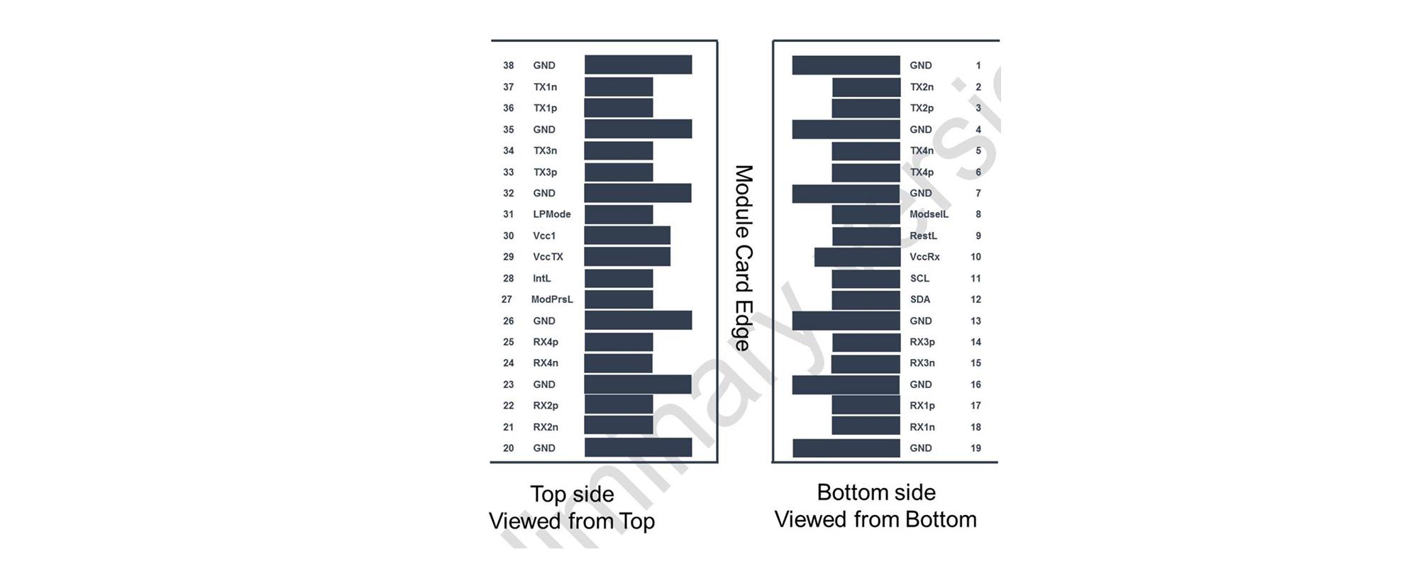
| PIN | Symbol | Description | Ref. | ||||||
| 1 | GND | Ground | – | ||||||
| 2 | TX2n | Transmitter Inverted Data Input | – | ||||||
| 3 | TX2p | TransmitterNon-Inverted Data Input | – | ||||||
| 4 | GND | Ground | ® | ||||||
| 5 | TX4n | Transmitter Inverted Data Input | – | ||||||
| 6 | TX4p | Transmitter Non-Inverted DataInput | – | ||||||
| 7 | GND | Ground | ® | ||||||
| 8 | ModSelL | Module Select | ® | ||||||
| 9 | ResetL | Module Reset | ® | ||||||
| 10 | VccRX | +3.3V Receiver Power Supply Receiver | – | ||||||
| 11 | SCL | 2-wire Serial Interface Clock | ® | ||||||
| 12 | SDA | 2-wire Serial Interface Data | ® | ||||||
| 13 | GND | Ground | ® | ||||||
| 14 | RX3p | Receiver Non-Inverted Data Output | – | ||||||
| 15 | RX3n | Receiver Inverted Data Output | – | ||||||
| 16 | GND | Ground | ® | ||||||
| 17 | RX1p | Receiver Non-Inverted DataOutput | – | ||||||
| 18 | RX1n | Receiver Inverted Data Output | – | ||||||
| 19 | GND | Ground | ® | ||||||
| 20 | GND | Ground | ® | ||||||
| 21 | RX2n | Receiver Inverted Data Output | – | ||||||
| 22 | RX2p | Receiver Non-Inverted Data Output | – | ||||||
| 23 | GND | Ground | ® | ||||||
| 24 | RX4n | Receiver Inverted Data Output | – | ||||||
| 25 | RX4p | Receiver Non-Inverted DataOutput | – | ||||||
| 26 | GND | Ground | ® | ||||||
| 27 | ModPrsL | Module Present,internal pulled down to GND | – | ||||||
| 28 | IntL | Interrupt output,should be pulled up on host board | – | ||||||
| 29 | VccTX | +3.3V Transmitter Power Supply | – | ||||||
| 30 | Vcc1 | +3.3V Power Supply | – | ||||||
| 31 | LPMode | LowPowerMode | ® | ||||||
| 32 | GND | Ground | – | ||||||
| 33 | TX3p | Transmitter Non-Inverted Data Input | – | ||||||
| 34 | TX3n | Transmitter Inverted Data Input | – | ||||||
| 35 | GND | Ground | – | ||||||
| 36 | TX1p | Transmitter Non-Inverted Data Input | – | ||||||
| 37 | TX1n | Transmitter Inverted Data Input | – | ||||||
| 38 | GND | Ground | ® | ||||||
| ① GND is the symbol for signal and supply (power) common for the module. All are common within the module and all module voltages are reference to this potential unless otherwise noted. Module circuit ground is isolated from module chassis ground within the module. ② Open collector, should be pulled up with 4.7~10K o hms on the host board to a voltage between 3.15V and 3.6V. |
|||||||||

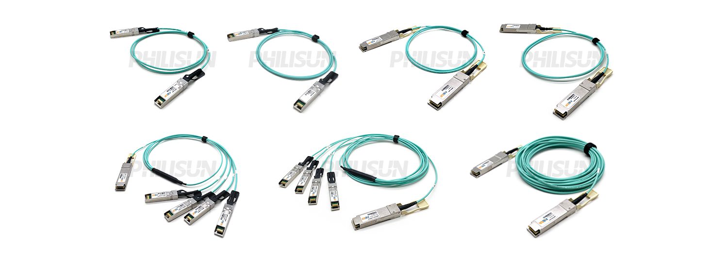
Related products
-

400G QSFP-DD to 2×200G QSFP56 Active Optical Cable(AOC)
Compliant with IEEE 802.3、QSFP-DD MSA、SFF-8024、SFF-8679、SFF-8665、OIF-CEI-04.0、CMIS 4.0 standard
Switch to Switch
Switch to GPU -

400G QSFP-DD to 4×100G QSFP56 Active Optical Cable(AOC)
Compliant with IEEE 802.3cd、OIF-CEI、QSFP-DD MSA、QSFP-DD-CMIS、IEEE 802.3bs Annex120E、SFF-8024、SFF-8679 standard
Switch to Switch
Switch to GPU -
")
400G QSFP-DD to QSFP-DD Active Optical Cable (AOC)
Compliant with theSFF-8436 QSFP-DD MSA standard
Switch to Switch
Switch to GPU -

400G QSFP-DD to 8×50G SFP56 Active Optical Cable(AOC)
Compliant with QSFP-DD MSA/SFP28 MSA和IEEE 802.3cd standard
Switch to Switch
Switch to GPU