

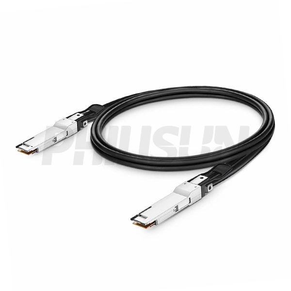
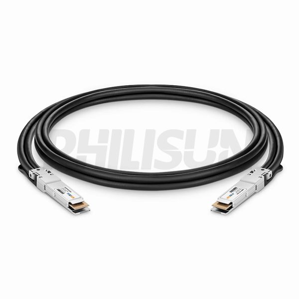

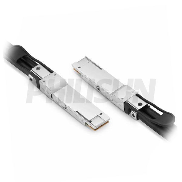
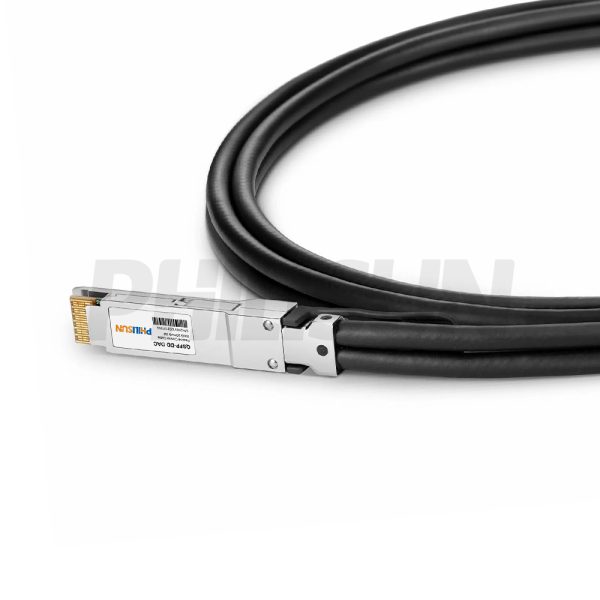
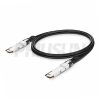
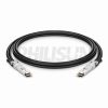
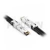
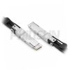
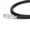
200G QSFP-DD to QSFP-DD Passive Direct Attach Copper Twinax Cable (DAC)
Compliant with IEEE 802.3bj, QSFP-DD MSA, CMIS, SFF-8417 standard
Switch to Switch
Switch to GPU
- High Quality
- Factory Outlet
- Satisfaction Guarantee
- Global Shipping
| SPECIFICATIONS | |||
|---|---|---|---|
| Cable End Connector A | QSFP-DD | Cable End Connector B | QSFP-DD |
| Jumper Type | Direct-Attach | Data Rate | 200G |
| Aggregate Bit Rate | 200Gbps | Lane Bit Rate | 25Gbps |
| Number of Channels | 8 | Single Channel Rate | 25G |
| Minimum Bend Radius | 5X Cable OD -Single, 10X Cable OD - Repeated | Factory Brand | PHILISUN |
| Attenuation | 28AWG:10dB/7m maximum 30AWG:8.4dB/5.5m maximum | Bit Error Rate | ≤10-12 |
| Shield | Braid/Foil | Wire AWG | 26AWG/30AWG |
| Cable Type | Passive Twinax | Cable OD | 30AWG: 6.9mm 28AWG: 8.1mm |
| Cable Colour/Material | Black PVC(OFNR) | Cable Length Selection | 0.5-3meter |
| Protocols | IEEE 802.3bj/QSFP-DD MSA/ CMIS/SFF-8417 | Application Scenarios | 200Gigabit Ethernet (200GbE) |
| Supply Voltage | 3.3V | Power Dissipation | <0.1W |
| Operating Temperature | 0 to 70℃ (32 to 158℉) | Storage Temperature | -40 to 85℃ (-40 to 185℉) |
PRODUCT PRESENTATION
The PHILISUN 200G QSFP-DD to QSFP-DD Passive Direct Attach Copper Twinax Cable (DAC) provides a robust, point-to-point link for 200 Gigabit Ethernet, optimized for high-density QSFP-DD architectures. It is fully compliant with IEEE 802.3bj, QSFP-DD MSA, and CMIS standards. This Passive Copper cable is an ideal, Cost-Effective solution for Low Latency connections over short distances, supporting direct Switch to Switch communication and critical Server Interconnect paths from Switch to GPU within the rack.
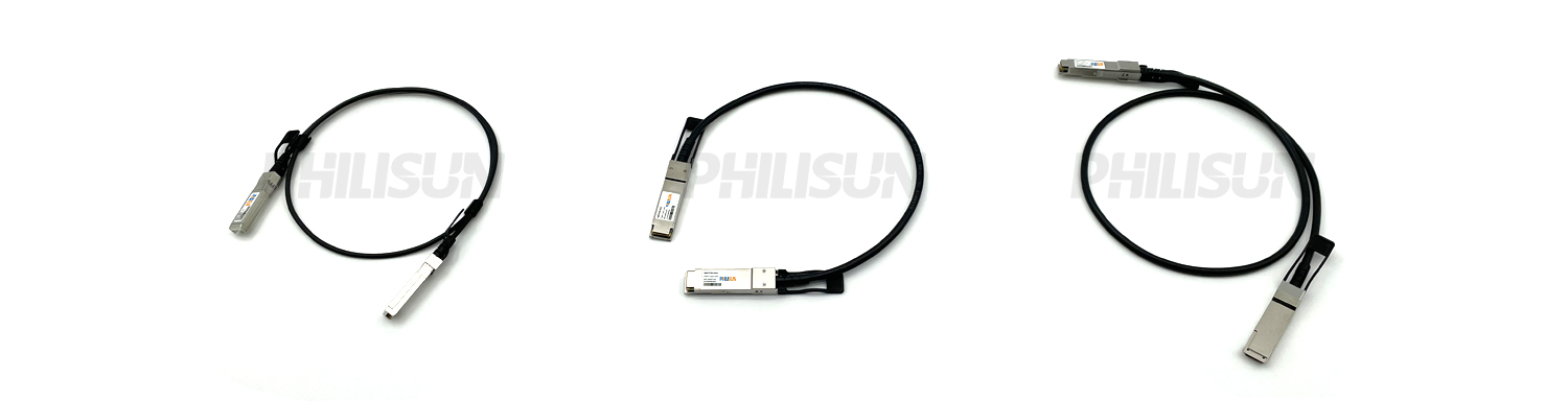
DAC SERIES PRODUCTS
PRODUCTION & TESTING EQUIPMENT

PERFORMANCE PARAMETER
| Recommended Operating Environment | |||||||||
| Parameter | Symbol | Min. | Typical | Max. | Unit | ||||
| Storage Temperature | – | -40 | – | +85 | ℃ | ||||
| Operating Case Temperature | TC | 0 | – | +70 | ℃ | ||||
| Power Supply Voltage | VCC3 | 3.135 | 3.3 | 3.465 | V | ||||
| Data Rate Per Lane | – | – | 200 | – | Gbps | ||||
| Electrical Characteristics | |||||||||
| Item | Parameter | Notes | |||||||
| Physical | Length | 0.5m, 1m, 1.5m, 2m, 2.5m, 3m | / | ||||||
| Cable Colour | Black | / | |||||||
| Backshell Material | Nickel Plated Zinc | / | |||||||
| Cable Jacket Material | Polyvinyl Chloride (PVC) | / | |||||||
| Minimum Bend Radius | 10x OD | / | |||||||
| Electrical | Resistance | 2 ohms Max. | / | ||||||
| Insulation Resistance | 10M ohms Min. | / | |||||||
| SI Performance | SDD21&SDD12 | -22.48 dB Min. | @12.89GHz | ||||||
| SDD11&SDD22 | -16.5+2*sqrt(f) dB Max. | @0.05GHz~4. 1GHz | |||||||
| -10.66+14*log(f/5.5) dB Max. | @4. 1GHz~10GHz | ||||||||
| SCD21-SDD21 | -10 dB Max. | @0.01GHz~12.89GHz | |||||||
| -27+(29/22)*fdB Max. | @12.89GHz~15.7GHz | ||||||||
| -6.3 dB Max. | @15.7GHz~19GHz | ||||||||
| Mechanical Performance | Mating Forces | QSFP-DD<90N | A rate of 10mm per minute | ||||||
| Un-mating Forces | QSFP-DD<50N | A rate of 10mm per minute | |||||||
| Latch Strength | Minimum of an 125N Force | Pull to separate module from cage, Test with connector, cage & module (latch engaged) |
|||||||
| Bulk cable retention in module |
Minimum of an 90N Force | Pull to separate bulk cable from module,Test with cable assembly only |
|||||||
| Wire Flex | No microsecond discontinuities are allowed. |
Flex cable 180° for 10 cycles at X/Y axis, 20 times/minutes, with an 1kg suspended weight. Type C EIA 364-41, test condition I. | |||||||
| Durability | No evidence of physical damage | Perform 50 unplug/plug cycles | |||||||
| Cable Minimum Bend Radius | No physical damage , Verify continuity and SI |
The cable is bent on time over the correct mandrel with 5 perpendicular, the Minimum bendRadius is 10x OD. | |||||||
PIN Definitions for QSFP-DD
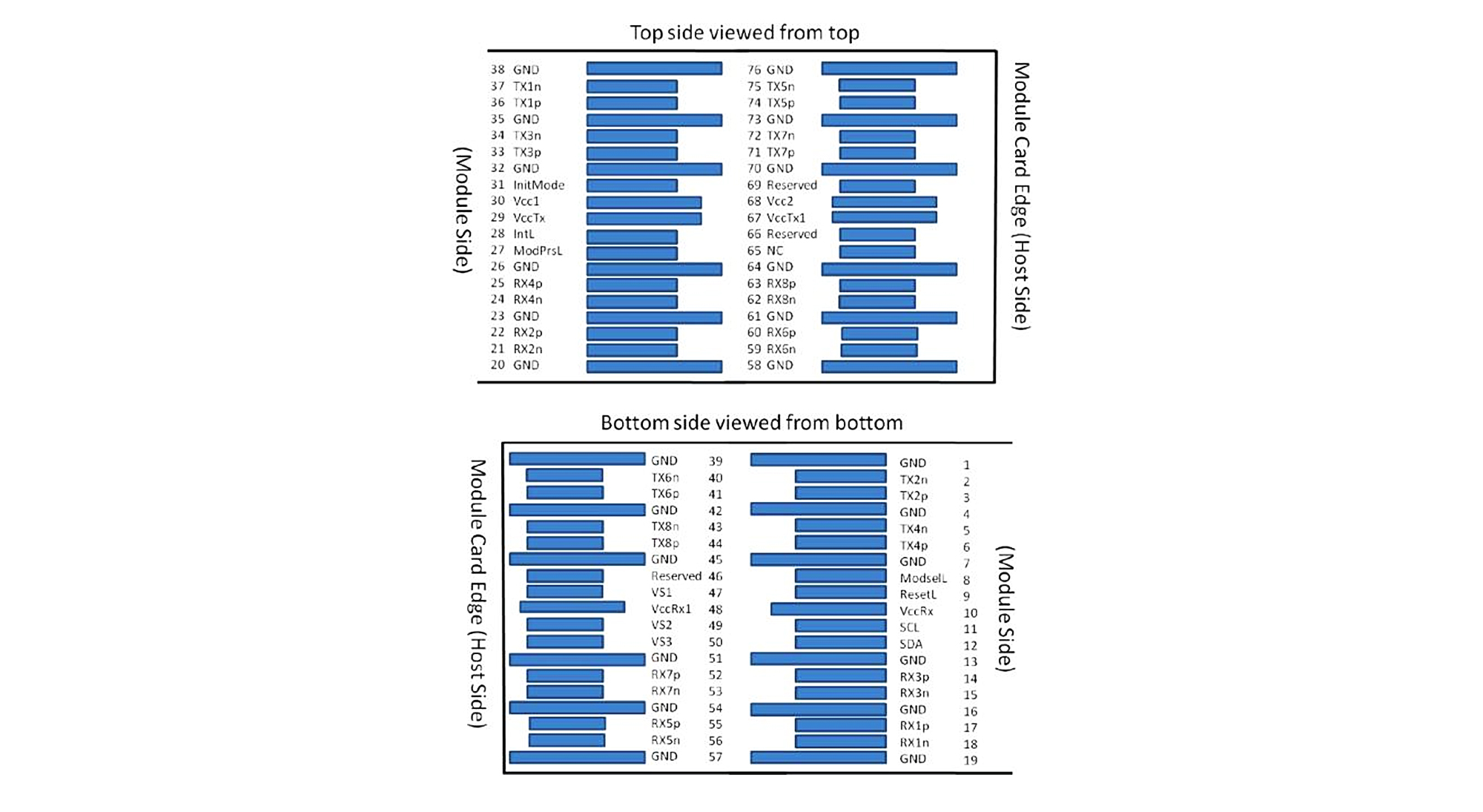
| PIN | Logic | Symbol | Name/Description | Notes | |||||
| 1 | – | GND | Ground | – | |||||
| 2 | CML-I | Tx2n | Transmitter Inverted Data Input | – | |||||
| 3 | CML-I | Tx2p | Transmitter Non-Inverted Data Input | – | |||||
| 4 | – | GND | Ground | 1 | |||||
| 5 | CML-I | Transmitter Inverted Data Input | Transmitter Inverted Data Input | – | |||||
| 6 | CML-I | Transmitter Non-Inverted Data Output | Transmitter Non-Inverted Data Input | – | |||||
| 7 | – | Ground | Ground | 1 | |||||
| 8 | LVTTL-I | Module Select | Module Select | – | |||||
| 9 | LVTTL-I | Module Reset | Module Reset | – | |||||
| 10 | – | Description | +3.3V Power Supply Receiver | 2 | |||||
| 11 | LVCMOS-I/O | 3.3V Power Supply Receiver | 2-wire serial interface clock | – | |||||
| 12 | LVCMOS-I/O | 2-Wire Serial Interface Clock | 2-wire serial interface data | – | |||||
| 13 | – | 2-Wire Serial Interface Data | Ground | 1 | |||||
| 14 | CML-O | Ground | Receiver Non-Inverted Data Output | – | |||||
| 15 | CML-O | Receiver Non-Inverted Data Output | Receiver Inverted Data Output | – | |||||
| 16 | – | Receiver Inverted Data Output | Ground | 1 | |||||
| 17 | CML-O | Ground | Receiver Non-Inverted Data Output | – | |||||
| 18 | CML-O | Receiver Non-Inverted Data Output | Receiver Inverted Data Output | – | |||||
| 19 | – | Receiver Inverted Data Output | Ground | 1 | |||||
| 20 | – | Ground | Ground | 1 | |||||
| 21 | CML-O | Ground | Receiver Inverted Data Output | – | |||||
| 22 | CML-O | Receiver Inverted Data Output | Receiver Non-Inverted Data Output | – | |||||
| 23 | – | Receiver Non-Inverted Data Output | Ground | 1 | |||||
| 24 | CML-O | Ground | Receiver Inverted Data Output | – | |||||
| 25 | CML-O | Receiver Inverted Data Output | Receiver Non-Inverted Data Output | – | |||||
| 26 | – | Receiver Non-Inverted Data Output | Ground | 1 | |||||
| 27 | LVTTL-O | Ground | Module Present | – | |||||
| 28 | LVTTL-O | Module Present | Interrupt | – | |||||
| 29 | – | Interrupt | +3.3V Power Supply Transmitter | 2 | |||||
| 30 | – | Description | +3.3V Power Supply | 2 | |||||
| 31 | LVTTL-I | 3.3 V Power Supply Transmitter | Initialization mode; In legacy QSFP applications, the InitMode pad is called LPMODE |
– | |||||
| 32 | – | 3.3 V Power Supply | Ground | 1 | |||||
| 33 | CML-I | Low Power Mode | Transmitter Non-Inverted Data Input | – | |||||
| 34 | CML-I | Ground | Transmitter Inverted Data Input | – | |||||
| 35 | – | Transmitter Inverted Data Input | Ground | 1 | |||||
| 36 | CML-I | Transmitter Non-Inverted Data Output | Transmitter Non-Inverted Data Input | – | |||||
| 37 | CML-I | Ground | Transmitter Inverted Data Input | – | |||||
| 38 | – | Transmitter Inverted Data Input | Ground | 1 | |||||
| 39 | – | Transmitter Non-Inverted Data Output | Ground | 1 | |||||
| 40 | CML-I | Ground | Transmitter Inverted Data Input | – | |||||
| 41 | CML-I | Tx6p | Transmitter Non-Inverted Data Input | – | |||||
| 42 | – | GND | Ground | 1 | |||||
| 43 | – | Tx8n | Transmitter Inverted Data Input | – | |||||
| 44 | – | Tx8p | Transmitter Non-Inverted Data Input | – | |||||
| 45 | – | GND | Ground | 1 | |||||
| 46 | – | Reserved | For future use | 3 | |||||
| 47 | – | VSl | Module Vendor Specific 1 | 3 | |||||
| 48 | – | VccRx1 | 3.3V Power Supply | 2 | |||||
| 49 | – | VS2 | Module Vendor Specific 2 | 3 | |||||
| 50 | – | VS3 | Module Vendor Specific 3 | 3 | |||||
| 51 | – | GND | Ground | 1 | |||||
| 52 | CML-O | Rx7p | Receiver Non-Inverted Data Output | – | |||||
| 53 | CML-O | Rx7n | Receiver Inverted Data Output | – | |||||
| 54 | GND | Ground | 1 | ||||||
| 55 | CML-O | Rx5p | Receiver Non-Inverted Data Output | – | |||||
| 56 | CML-O | Rx5n | Receiver Inverted Data Output | – | |||||
| 57 | – | GND | Ground | 1 | |||||
| 58 | – | GND | Ground | 1 | |||||
| 59 | CML-O | Rx6n | Receiver Inverted Data Output | – | |||||
| 60 | CML-O | Rx6p | Receiver Non-Inverted Data Output | – | |||||
| 61 | – | GND | Ground | 1 | |||||
| 62 | CML-O | Rx8n | Receiver Inverted Data Output | – | |||||
| 63 | CML-O | Rx8p | Receiver Non-Inverted Data Output | – | |||||
| 64 | – | GND | Ground | 1 | |||||
| 65 | – | NC | No Connect | 3 | |||||
| 66 | – | Reserved | For future use | 3 | |||||
| 67 | – | VccTx1 | 3.3V Power Supply | 2 | |||||
| 68 | – | Vcc2 | 3.3V Power Supply | 2 | |||||
| 69 | – | Reserved | For future use | 3 | |||||
| 70 | – | GND | Ground | 1 | |||||
| 71 | CML-I | Tx7p | Transmitter Non-Inverted Data Input | – | |||||
| 72 | CML-I | Tx7n | Transmitter Inverted Data Input | – | |||||
| 73 | – | GND | Ground | 1 | |||||
| 74 | CML-I | Tx5p | Transmitter Non-Inverted Data Input | – | |||||
| 75 | CML-I | Tx5n | Transmitter Inverted Data Input | – | |||||
| 76 | – | GND | Ground | 1 | |||||
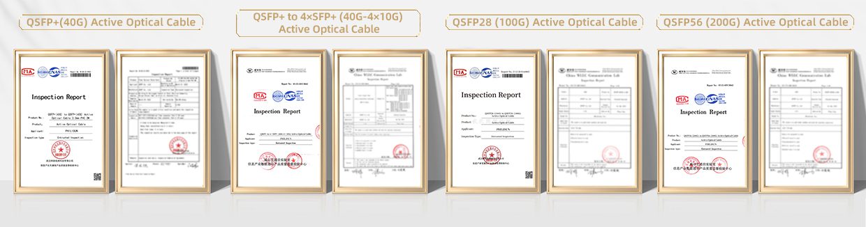
PRODUCT CERTIFICATION
COMPATIBLE BRANDS

CONFIGURATION INFORMATION
Related products
-

200G QSFP-DD to 2×100G QSFP28 Passive Direct Attach Copper Twinax Cable (DAC)
Compliant with QSFP-DD MSA、SFF-8661、IEEE 802.3bs-200GAUI-8、IEEE802.3bm-CAUI-4、CMIS 4.0、SFF-8636 standard
Switch to Switch
Switch to GPU